
Bandpass filter
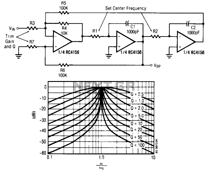
The frequency response for different values of Q is illustrated.
The circuit in question features a summing amplifier configuration, which is a fundamental building block in analog signal processing. The input signal is routed through resistor R3 to the inverting input of the operational amplifier (op-amp) configured as a summing amplifier. This configuration allows for the combination of multiple input signals, resulting in a single output that is proportional to the weighted sum of the inputs.
The op-amp maintains virtual ground at the inverting terminal, which means that the voltage at this terminal is kept equal to the voltage at the non-inverting terminal. This characteristic is critical for ensuring that the summation is accurate and that the output reflects the intended signal processing.
The output of the summing amplifier is connected to the first integrator stage. An integrator circuit typically consists of an op-amp, a feedback capacitor, and an input resistor. The integration process transforms a voltage signal into a current signal, effectively performing mathematical integration over time. This is particularly useful in applications such as signal smoothing, waveform shaping, and generating ramp signals.
The parameters defined in the circuit, specifically 1/R1C1 as 1 and 1/R2C2 as u>2> th^, are instrumental in determining the frequency response of the filter. The center frequency (ω0) and quality factor (Q) are essential in characterizing how the filter responds to different input frequencies. The quality factor is a dimensionless parameter that describes the bandwidth of the filter relative to its center frequency, with higher Q values indicating a narrower bandwidth and sharper resonance.
The frequency response of the circuit can vary significantly with different Q values, which can be analyzed graphically. This analysis allows for the adjustment of the circuit parameters to achieve desired filtering characteristics, making it a versatile tool in the design of analog filters and signal processing applications.The input signal is applied through R3 to the inverting input of the summing amplifier and the output is taken from the first integrator. The summing amplifier will maintain equal voltage at the inverting and non-inverting inputs. Defining 1/R1C1 as 1 and 1/R2C2 as u>2> th^ is now a convenient form to look at the center-frequency 0 and filter Q.
The frequency response for various values of Q is shown. 🔗 External reference
Related Circuits
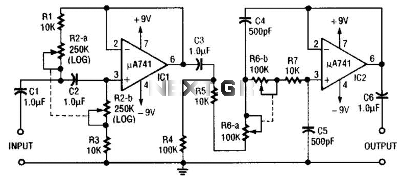
This circuit is a variable audio bandpass filter that features a low cutoff adjustable from approximately 25 Hz to 700 Hz and a high cutoff adjustable from 2.5 kHz to over 20 kHz. The roll-off is set at 12...
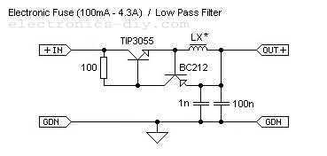
This is adjustable electronic fuse that can be used to protect power supplies from short circuits or can be also used to limit the current usage. It can be adjusted for currents from 100mA up to 4.3A. An adjustable electronic...
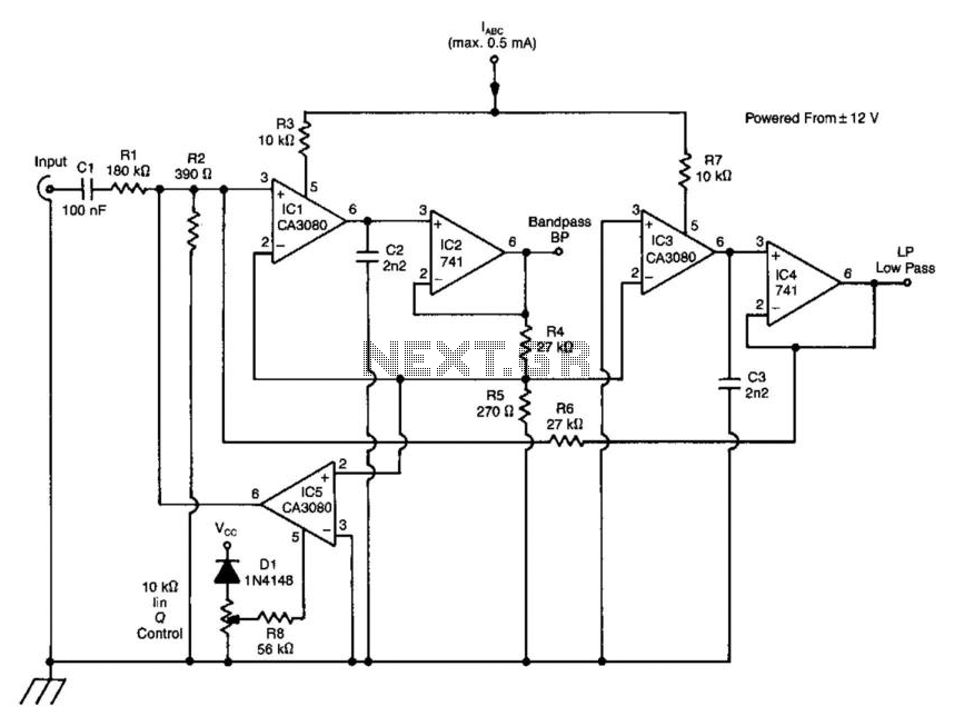
A standard dual integrator filter can be constructed using a few CA3080 operational amplifiers. By varying the parameters L, A, B, and C, the resonant frequency can be swept over a range of 1000:1. At IC1, three current-controlled integrators...
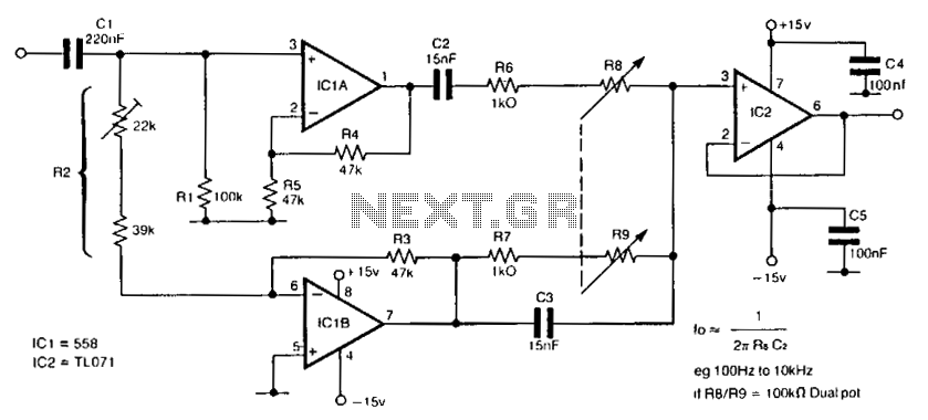
The circuit utilizes a single dual-ganged potentiometer to achieve tuning across a broad spectrum, potentially covering the entire audio range in a single adjustment. The underlying principle is based on the Wien bridge configuration, which is supplied with anti-phase...
What is a circuit breaker? When is an AC power line filter or a phone line filter necessary? How can a noise filter be designed? Is it possible to create a homemade surge protector? The following circuit protection options...
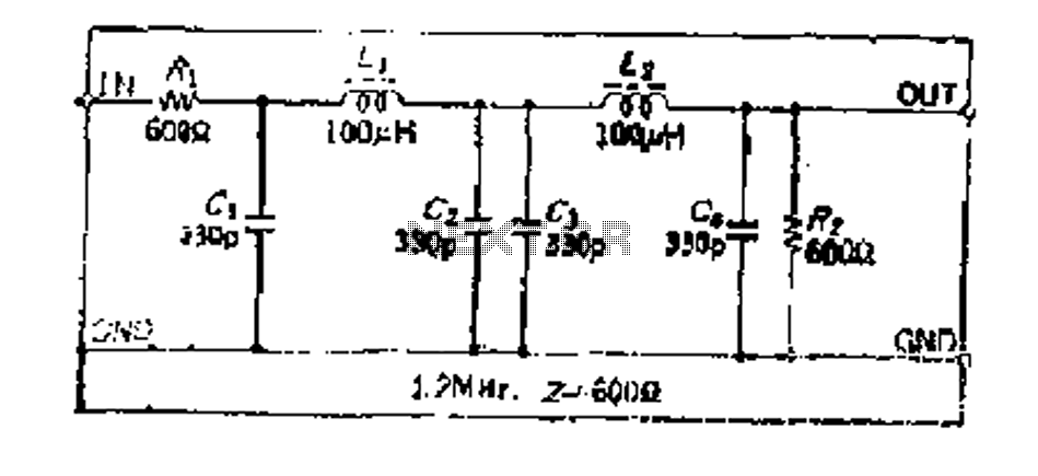
Due to the amplifier's frequency characteristics and the impact of parasitic capacitance, designing an active filter that operates effectively at hundreds of kilohertz is quite challenging. Additionally, since the circuit consists of a low-pass filter with a large coil...