
build own pabx
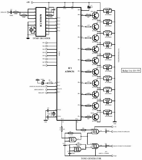
The circuit described operates on a primary 220V AC power source, which is transformed into lower voltages suitable for various functions within the telephone system. The step-down process involves using a transformer or a power supply module to achieve the required 24V and 72V outputs. The 18V DC is specifically utilized for powering the telephone components, ensuring that the system operates efficiently.
The ringing mechanism is controlled by a relay (RL10), which is responsible for activating the ringing bells using the 72V AC supply. The conversion of incoming bell signals into pulses is a critical function, allowing the system to recognize the ringing pattern and manage call handling effectively. The Timer1 in the microcontroller plays a crucial role in pulse counting to determine when to hold the call.
The use of the CD4093 integrated circuit allows for the generation of different tones. The oscillation frequencies produced by gates A and B are combined in gate C, leading to the generation of both the dial tone and busy tone. The control of these tones via specific microcontroller pins (P3.6 for dial tone and P3.4 for busy tone) ensures that the system can adaptively respond to user interactions.
The dual functionality of the opto-triac (IC5) as a hook switch is essential for managing call states. It allows the system to hold incoming calls and transmit melodies when the line is in use. The choice of using the UM66 melody IC instead of a voice recording chip reflects a practical solution to component availability issues, while still providing a pleasant user experience.
The circuit's design incorporates separate power sources for the speech and standby buses to prevent cross-talk and ensure privacy during conversations. This is particularly important in telecommunication systems where confidentiality is paramount. The MT8870 decoder is a vital component that interprets DTMF signals, enabling the system to recognize user inputs through the telephone keypad. The microcontroller processes these inputs, providing feedback through the indicators connected to Port2, which visually represent the status of each telephone set.
Overall, this circuit design demonstrates a comprehensive approach to managing telephone communication, combining power management, tone generation, and DTMF decoding in a cohesive and functional system.The main power source is 220V AC, which is step-down into 24V and 72V. The18V DC is used for telephone system and 72V AC supply is used for ringing telephone bells which is controlled by RL10. This stage converts the incoming bell signals into pulses. These pulses are counted by Timer1 in the micro controller. The system hold the (Outer) call afte r two bells, two bells have 37 pulses. This stage consists of CD4093. The gate A oscillate on 440Hz and gate B oscillate on low frequencies then gate C AND the output of A and B gate. This arrangement is done for generating dial tone and busy tone. Gate D generate dial tone, dial tone is controlled by P3. 6 and busy tone is controlled by P3. 4. Dial tone is provided to speech bus and busy tone is provide on standby bus. In this stage IC5 (Opto-triac) serves as hook switch, controlled by P1. 6. This stage perform dual function. First hold incoming call (From out side) and second transmit recorded voice massage (Melody) on telephone line.
I decide to use Voice recording/playing chip but unfortunately this was not available in local market, so I have used UM66 (Melody IC) instead of Voice recording chip which is controlled by P3. 7. This melody transmit to holding circuit through C10. If possible let you use any voice Recording/Playing module with some changes. There are two supply sources are used through gyrator, one for speech bus and other for stand-by bus.
This arrangement was necessary to make sure complete privacy during speech. If the same source was used for both buses, it was possible the speech transfer to the stand-by bus. The heart of this stage is IC2 (MT 8870). This IC decodes the DTMF input in the binary format. The output of decoder is provided to Port1 of the microcontroller. When a valid DTMF receive MT8870 strobe for 20msec to microcontroller on P1. 4. There are eight indicators are used, one for each telephone set, all indicator are attached to Port2. When some one is pickup the hand set of his telephone, the current is flow from the telephone via R26, some voltage are dropped on the resistance, which activate the relevant transistor hence logic low occur on his collector.
This logic is read by microcontroller on Port 2. 🔗 External reference
Related Circuits
This is a single transistor pump circuit. It is a straightforward circuit that is quite useful and can serve as a foundational component for designing more complex electronic systems. The single transistor pump circuit utilizes a transistor as the primary...
This up/down timer was designed to control a power antenna on a late-model vehicle. Normally, this vehicle uses a body computer to control the antenna. However, the owner intended to install a high-powered audio stereo system. The original stereo...
The voltage requirement for the Solidus is significantly higher than what your circuit currently provides. The Solidus device operates at a voltage level that exceeds the specifications of the existing circuit. To accommodate this requirement, circuit modifications will need to...
A 10-light LED bar graph is desired, where the LEDs light up sequentially until all are lit, then cycle back down until all are off. The LM3914 - Dot/Bar Display Driver is a simpler analog solution that operates in...
The circuit is designed for individuals who spend extensive hours exploring the various resources of this site. Although it comprises only three components, it effectively indicates whether the telephone line has been released after a prolonged connection via modem...

For the wiring of the display, the ribbon cable is first taken and soldered according to the circuit diagram on the 25-pin sub-D (parallel port) plug. The small circuit diagram illustrates the rear side, which is the solder side...
Warning: include(partials/cookie-banner.php): Failed to open stream: Permission denied in /var/www/html/nextgr/view-circuit.php on line 713
Warning: include(): Failed opening 'partials/cookie-banner.php' for inclusion (include_path='.:/usr/share/php') in /var/www/html/nextgr/view-circuit.php on line 713