
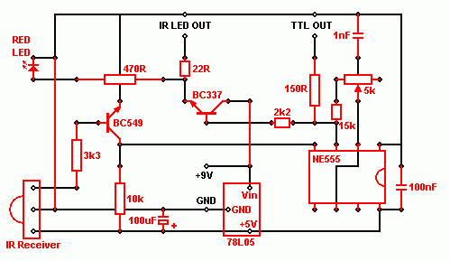
DIY computer infrared interface

The circuit includes two common contacts, A and B, which are typically used for establishing connections in various electronic applications. These contacts are illustrated in an outline drawing, which serves as a visual reference for their layout and connectivity. The pin definitions associated with these contacts are crucial for ensuring correct wiring and functionality within the circuit.
Component C is an infrared emission tube, which is utilized for transmitting infrared signals. The shape of the tube is critical for its performance, as it determines the angle and intensity of the emitted infrared light. The pin definitions for this component specify the connections required for proper operation, while the schematic symbol provides a standardized representation for inclusion in circuit diagrams.
The CD4069 component is a hex inverter, which contains six independent inverter gates. Each gate inverts the logic state of its input signal. The pin definitions for the CD4069 are essential for correctly interfacing with other components in the circuit, ensuring that signals are processed accurately.
Component F is a 9013 transistor, which is a NPN bipolar junction transistor commonly used for switching and amplification purposes. The shape of the 9013 transistor, along with its pin definitions, is important for understanding its configuration within a circuit. The schematic symbol for the transistor provides a visual representation that aids in circuit design and analysis.
This comprehensive description of the components and their functions facilitates a better understanding of the overall circuit design and aids in effective implementation and troubleshooting.A, B are 2 common contact, outline drawing and pin definition. C is the infrared emission tube shape, pin definition and schematic symbol. CD4069 is the pin definition of inverter pin, and F is the 9013 transistor shape, pin definitions and symbol.. 🔗 External reference
Related Circuits

Cable and xDSL modems are increasingly popular, leading to a need for designs that interface with existing telephones at subscriber locations. The subscriber line interface circuit (SLIC) within the modem must ring the phone and provide loop current during...
Here are a few details on the Infrared Remote Control Extender unit designed and built to control the NAD T752 A/V receiver. The NAD T752 features an IR input socket at the back, intended for installations where the unit...
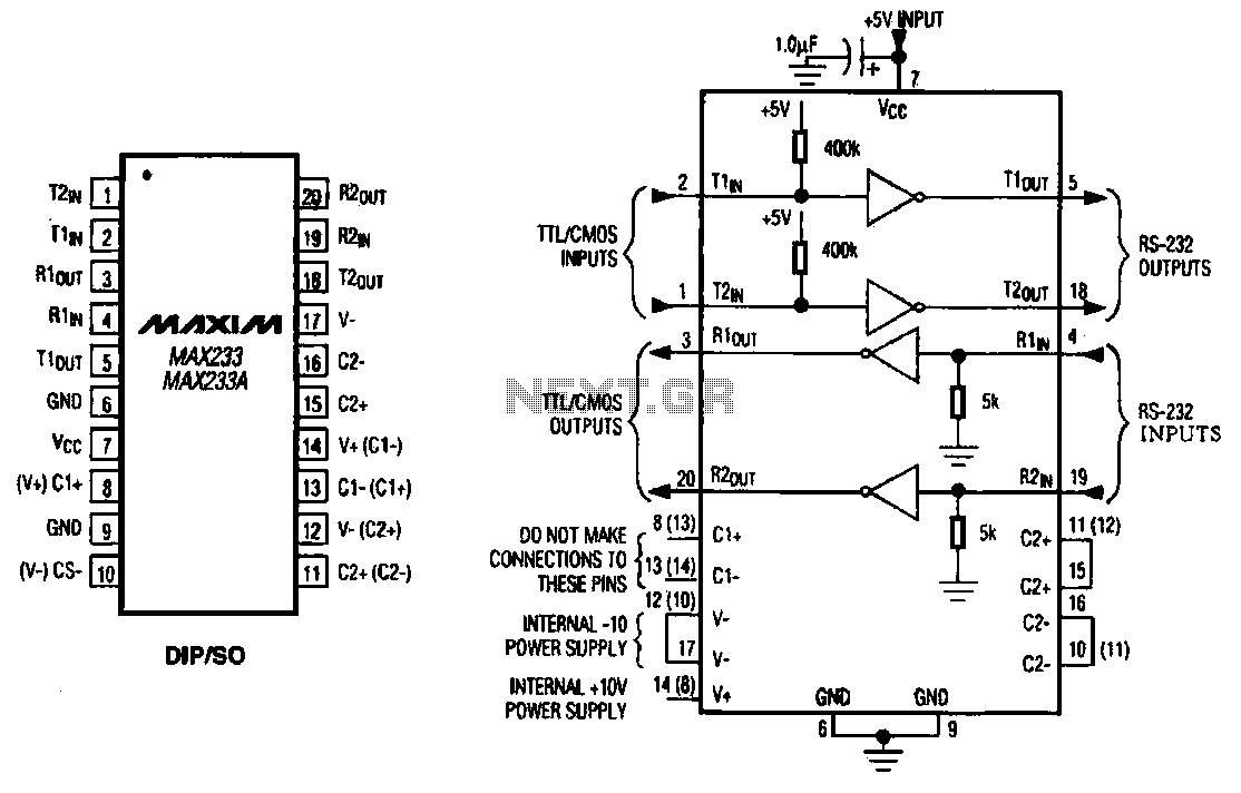
The MAX233 / 233A is a multi-channel data interface circuit featuring dual output and dual input driver circuits. It is designed for small digital products and multimedia equipment to facilitate data transmission. The MAX233 / 233A integrates multiple functions to...
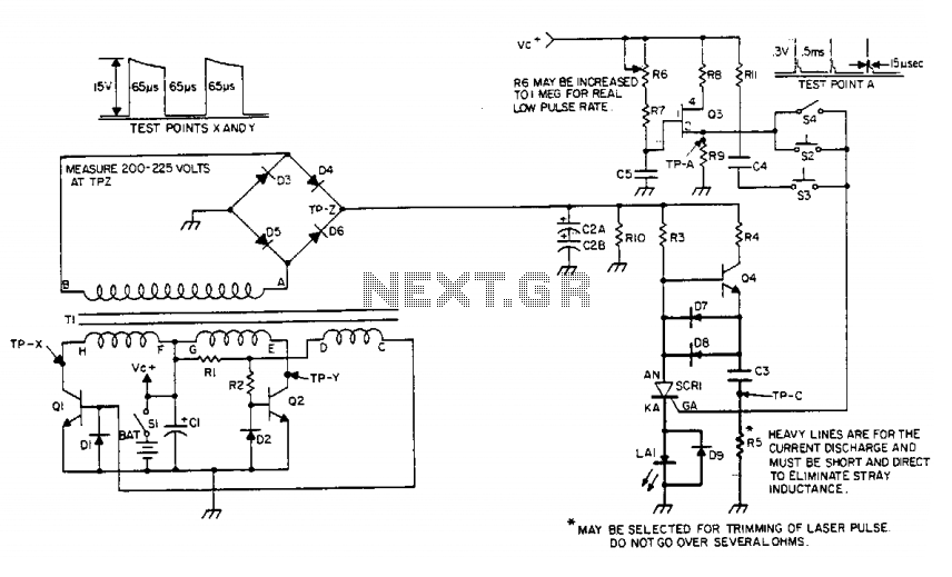
The device generates an adjustable frequency of low to medium powered infrared (IR) pulses of invisible energy and must be handled with care. The portable battery pack is stepped up to 200 to 300 volts by the inverter circuit,...
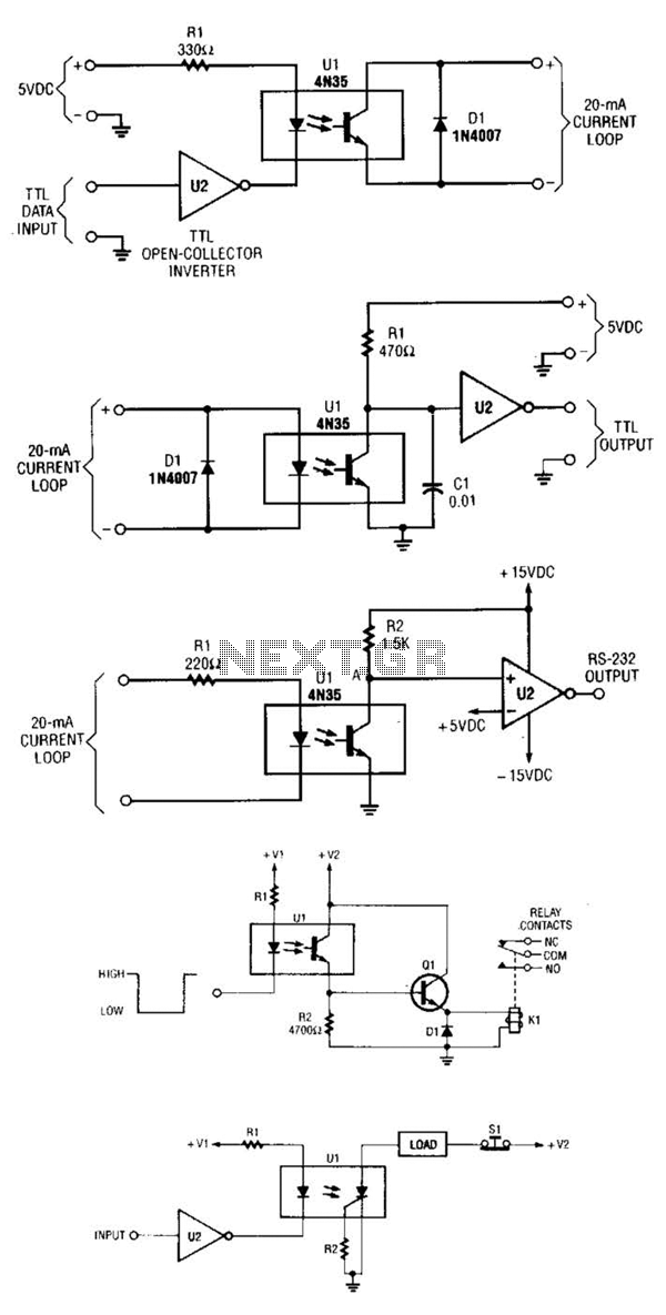
A circuit for isolating a variable resistor is presented. An optoisolator, which consists of an LED and a photo-conductive cell (or photoresistor), is utilized. The current flowing through the LED regulates its brightness, which subsequently dictates the resistance between...

The pyroelectric infrared sensor head operates as illustrated in the accompanying figure. Upon detecting an infrared signal from a human body within its monitoring zone, the sensor head generates a positive pulse signal. This signal is transmitted to the...
Warning: include(partials/cookie-banner.php): Failed to open stream: Permission denied in /var/www/html/nextgr/view-circuit.php on line 713
Warning: include(): Failed opening 'partials/cookie-banner.php' for inclusion (include_path='.:/usr/share/php') in /var/www/html/nextgr/view-circuit.php on line 713