
Precision Clock Generator
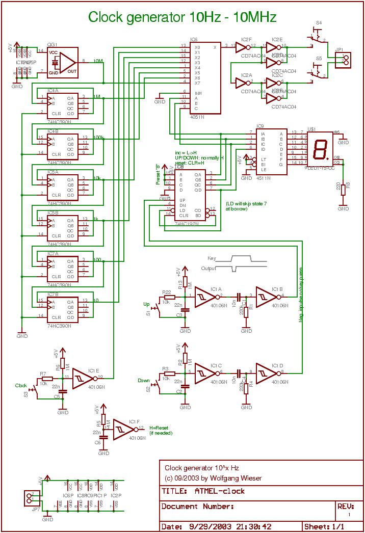
The clock generator circuit is designed to provide a versatile and efficient method for generating clock signals across a wide frequency range. The architecture primarily employs a 4051 multiplexer, which is pivotal for selecting the desired frequency based on the binary inputs provided by the pins A, B, and C. The use of push buttons S1 and S2 allows for intuitive user interaction, enabling easy frequency adjustments. The cascading configuration of the 74HC390 chips facilitates division of the input frequency, ensuring that the generator can produce a wide variety of output frequencies while maintaining signal integrity.
The inclusion of the CD40106 for switch debouncing is a critical design element, as it enhances the reliability of the user interface by preventing erroneous signal transitions caused by mechanical bounce in the push buttons. The design of the impulse generation through IC1B and IC1D ensures that the user experiences immediate feedback when adjusting the frequency, aligning with user expectations for responsive control.
The output stage, utilizing 74AC04 inverters, is engineered to deliver robust drive capability, making it suitable for interfacing with various loads. The consideration of signal propagation delay due to the unequal number of inverters for the complementary signals is a thoughtful approach in ensuring that the overall performance of the clock generator remains within acceptable limits for most applications.
Overall, the design reflects a balance between functionality and practicality, with careful attention given to user interaction, signal integrity, and circuit simplicity. This clock generator serves as a valuable tool for applications requiring precise timing signals, whether in experimental setups or integrated into larger electronic systems.The device presented here can generate a complementary clock signal at frequencies of 10Hz to 10MHz in steps of factor10. Thus, I chose to call it "10xHz clock generator" (with x being a number between 1 and 7). It can also be used to manually create clock impulses using a press button. The frequency is selected using two press buttons/swiches: S1 to switch the frequency up by a factor of 10 and S2 to switch it down. The frequency selection is determined by the three pins A, B, C at the 4051 which are just the binary representation of the x-value. 7 (i. e. A, B, C being HIGH) selects the direct signal from the crystal-controlled oscillator OG1 while lower numers/combinations select lower frqeuencies from the divide-cascade built-up with three 74HC390 chips.
Note that when pressing the "up" button when value 7 is active will switch back to value "0" (i. e. manual clocking, see below) while pressing down at value "0" will step to 6 instead of 7. I knew this bug before building the circuit but I decided that implementing the correct behavior was not worth the additional circuicy. The CD40106 is used to debounce the switches. Especially note IC1B and IC1D which form a small negative impulse when pressing the up/down key. This is needed to make the frequency change when pressing the switch instead of when releasing it which would be counter-intuitive/unexpected behaviour.
The output stage is done with two parallel 74AC04 inverters which can source and sink up to 24mA each with slew rates at least as good as the HC family. Due to the fact that the complementary signals travel through a different number of inverters, they are not exactly in sync but the delay of about <7ns should not make big trouble.
Note: The design above leaves away all the bypassing capacitors. That is because I chose to solder them directly on the IC socket pins for optimum performance and because otherwise the required signal lines proved to make PCB design much more complicated in the past. 🔗 External reference
Related Circuits
The nixie tube clock consists of a high-voltage power supply, seven ring counters, and an Atmel AVR processor. The power supply is shown in Schematic 1. It takes 12 volts AC and converts it to DC, which drives the...

This Project is made up with AT89C2051 and the RTC DS1307. It has a large Seven segment display. The standard remote control is used to change the Time. More: Procedure to enter the Time 1. Press power button on...
A measure delay generator, also identified similarly to a sequence generator, is a device that provides output signals at specified time intervals from a time reference. It automatically resets when the input signal returns to ground. The schematic illustrates...
This regulator is designed to control a DC generator. In this configuration, one side of the field is grounded. Diode D4 prevents the battery from discharging through the generator and serves as a replacement for the mechanical cut-out relay....

The voltage rating of the 470 µF capacitor is not critical, provided it significantly exceeds the maximum power supply voltage, which is 12 volts in this circuit. It is essential to connect this capacitor correctly, observing its polarity. The...
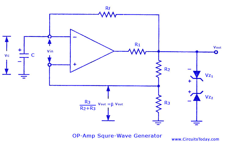
Non-sinusoidal waveform generators are also referred to as relaxation oscillators. The op-amp relaxation oscillator depicted in the figure functions as a square wave generator. Generally, square waves are relatively simple to generate. Similar to the UJT relaxation oscillator, the...
Warning: include(partials/cookie-banner.php): Failed to open stream: Permission denied in /var/www/html/nextgr/view-circuit.php on line 713
Warning: include(): Failed opening 'partials/cookie-banner.php' for inclusion (include_path='.:/usr/share/php') in /var/www/html/nextgr/view-circuit.php on line 713