
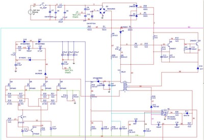
Inductive switching power supply circuit diagram
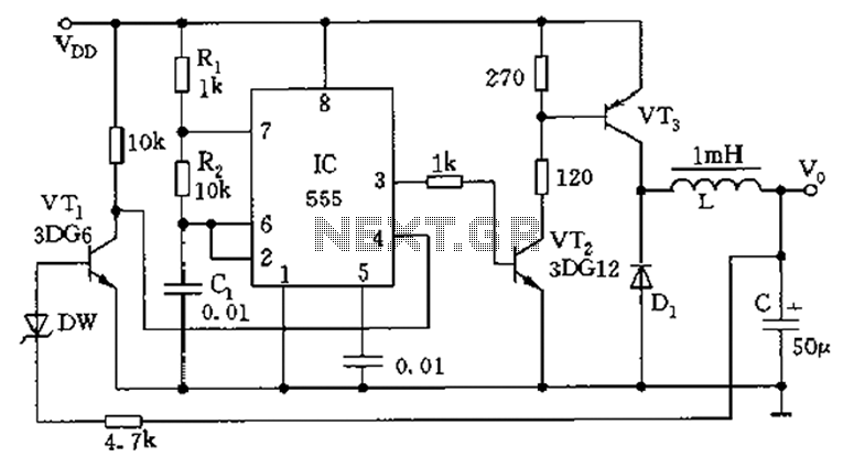
The described circuit utilizes a 555 timer in an astable configuration, which continuously switches between high and low states, thus generating a square wave output. The timing components, R1, R2, and C1, dictate the frequency and duty cycle of the oscillation. The output frequency of around 10 kHz is suitable for various applications, including pulse width modulation (PWM) and signal generation.
Transistors VT2 and VT3 are employed to manage the current flow effectively. When the output from the 555 timer is high, these transistors are turned on, allowing current to flow through the inductor (L). This action causes the inductor to store energy in its magnetic field. As the output transitions to low, the inductor releases its stored energy, which is directed to the load via a freewheeling diode. This diode prevents back EMF generated by the inductor from damaging the circuit components, ensuring safe operation.
The circuit also incorporates protective measures against overvoltage conditions. When the voltage exceeds a predetermined threshold, the breakdown of diode DW triggers the saturation of transistor VT1. This causes a significant drop in voltage at point C, effectively resetting the 555 timer and halting the oscillation. This feature is crucial for maintaining the stability of the circuit and preventing damage due to excessive voltage levels.
Overall, this circuit design exemplifies a robust method for generating oscillations while incorporating current management and protective features, making it suitable for various electronic applications requiring precise timing and regulation.As illustrated, 555 and R1, R2, C1 composition astable multivibrator, the oscillation frequency is about 10kHz, duty cycle close to 50%. VT2, VT3 switch as expanding the use of current use. When the square wave oscillator is high, VT2, VT3 conduction, the LC discharge; is low, L energy storage through freewheeling diode circuit power supply to the load. When overvoltage, DW breakdown, VT1 saturated conduction, c was very low ( 0.7V), 555 reset to stop, play the role of regulator and dynamic balance.
Related Circuits
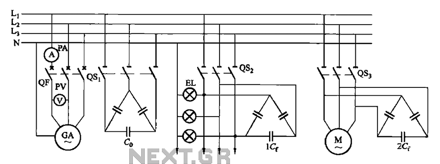
A three-phase squirrel cage induction motor is driven by a prime mover (such as diesel engines) and has asynchronous motor stator windings connected to the output end along with several capacitors for excitation power, enabling it to produce three-phase...
An ultrasonic cleaner is effective for cleaning specific items. This circuit employs a microcontroller to manage timing and provide a digital display, although a basic oscillator can be utilized if preferred. RESL and RES2 are piezoelectric transducers activated by...
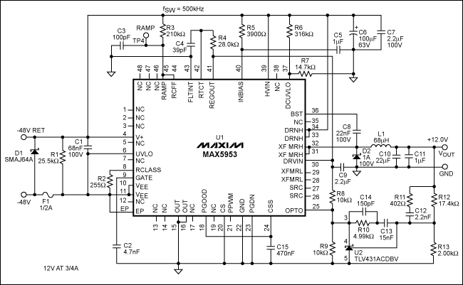
The MAX5953A offers a straightforward, cost-effective, and comprehensive non-isolated power integrated circuit (IC) solution for Powered Devices (PD) in Power-over-Ethernet (PoE) systems. The MAX5953A is designed to facilitate the implementation of Power-over-Ethernet applications by providing an efficient means of...
A Power Factor Correction (PFC) board has been obtained from an old Sun Microsystems Spark450 power supply (part number 300-1359-xx). This board contains all necessary components for a 650-watt inverter. However, the complete PFC circuit is not fully detailed...
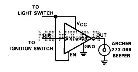
The SN75604, which features input control logic and requires only a single supply rail, can be utilized in light activation sensors and alarm drivers. The device's Vqq and enable inputs are connected to a voltage lead from the light...

The reflectometer (SWR power meter) operates across three decades, ranging from 100 kHz to 100 MHz. It can be designed to handle RF power levels as low as 500 mW and up to 500 watts. The reflectometer, also known as...
Warning: include(partials/cookie-banner.php): Failed to open stream: Permission denied in /var/www/html/nextgr/view-circuit.php on line 713
Warning: include(): Failed opening 'partials/cookie-banner.php' for inclusion (include_path='.:/usr/share/php') in /var/www/html/nextgr/view-circuit.php on line 713