
0-30V Stabilized Variable Power Supply with Current Control
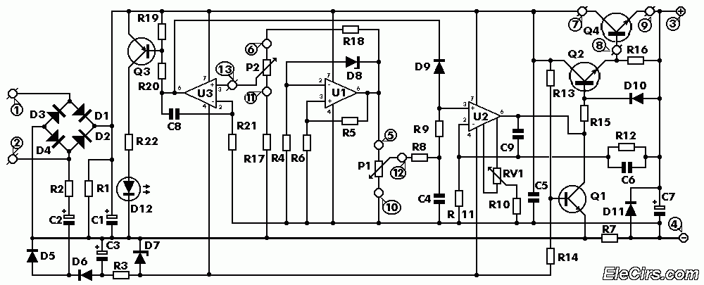
The power supply circuit described is designed to provide a reliable and adjustable output voltage and current, making it suitable for various applications. The step-down transformer is a critical component, as it ensures that the voltage is safely reduced from mains levels to usable low voltage levels. The rectification process, achieved through the diode bridge, converts the AC voltage from the transformer into DC voltage. The smoothing filter, consisting of the capacitor and resistor, plays a vital role in eliminating ripple voltage, ensuring a stable DC output.
The unique approach of using a constant gain amplifier for voltage regulation enhances the stability and precision of the power supply. The Zener diode serves as a reference voltage source, ensuring that fluctuations in the output are minimized. The configuration of resistors R5 and R6, along with the operational amplifier, facilitates a predictable and stable output voltage that is easily adjustable. The amplification stage provided by U2 further increases the voltage to the required levels, while the adjustment components (RV1 and R10) ensure that the output can be finely tuned to meet specific requirements.
This power supply circuit is ideal for laboratory use, testing, and other applications where adjustable DC voltage and current are necessary. The design emphasizes stability, precision, and versatility, making it a valuable addition to any electronics workbench.This is high quality stabilized power supply circuit diagram. You will able to adjust the output voltage from 0 volt up to 30 volt DC. You also able to adjust the current output value from 0. 002 A to 3 A. To start with, there is a step-down mains transformer with a secondary winding rated at 24 V/3 A, which is connected across the input points of the circuit at pins 1 & 2. (the quality of the supplies output will be directly proportional to the quality of the transformer). The AC voltage of the transformers secondary winding is rectified by the bridge formed by the four diodes D1-D4.
The DC voltage taken across the output of the bridge is smoothed by the filter formed by the reservoir capacitor C1 and the resistor R1. The circuit incorporates some unique features which make it quite different from other power supplies of its class.
Instead of using a variable feedback arrangement to control the output voltage, our circuit uses a constant gain amplifier to provide the reference voltage necessary for its stable operation. The reference voltage is generated at the output of U1. The circuit operates as follows: The diode D8 is a 5. 6 V zener, which here operates at its zero temperature coefficient current. The voltage in the output of U1 gradually increases till the diode D8 is turned on. When this happens the circuit stabilises and the Zener reference voltage (5. 6 V) appears across the resistor R5. The current which flows through the non inverting input of the op-amp is negligible, therefore the same current flows through R5 and R6, and as the two resistors have the same value the voltage across the two of them in series will be exactly twice the voltage across each one.
Thus the voltage present at the output of the op-amp (pin 6 of U1) is 11. 2 V, twice the zeners reference voltage. The integrated circuit U2 has a constant amplification factor of approximately 3 X, according to the formula A=(R11+R12)/R11, and raises the 11. 2 V reference voltage to approximately 33 V. The trimmer RV1 and the resistor R10 are used for the adjustment of the output voltages limits so that it can be reduced to 0 V, despite any value tolerances of the other components in the circuit.
🔗 External reference
Related Circuits
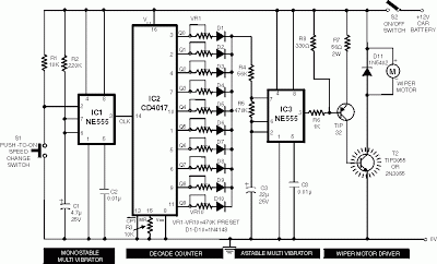
The circuit includes a momentary switch S1 that triggers an alarm pulse for the decade counter IC2, which increments its count with each alternating alarm pulse or the activation of switch S1. Ten variable resistors (VR1 through VR10) are...

The generated alternating current (AC) at both ends of the voltage is adjusted after being rectified to supply the motor armature windings, allowing for speed adjustments of a 15W lamp. It is noteworthy that despite the freewheeling role of...
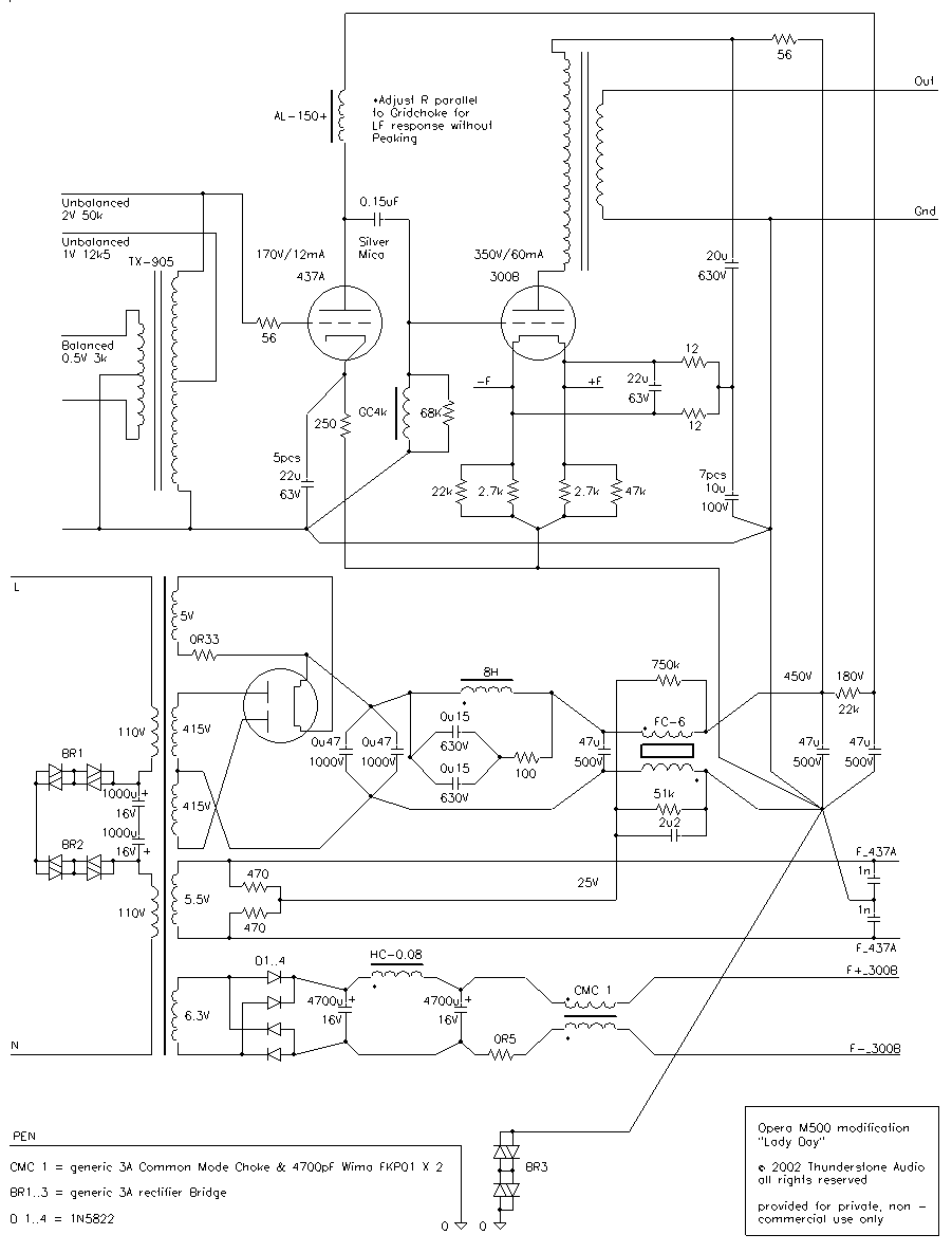
A request for a DIY 300BSE power amplifier schematic is made, with a specification to utilize Lowther PM6 speakers. The 300BSE power amplifier is a well-regarded audio amplification circuit known for its warm sound and high fidelity, particularly suited for...
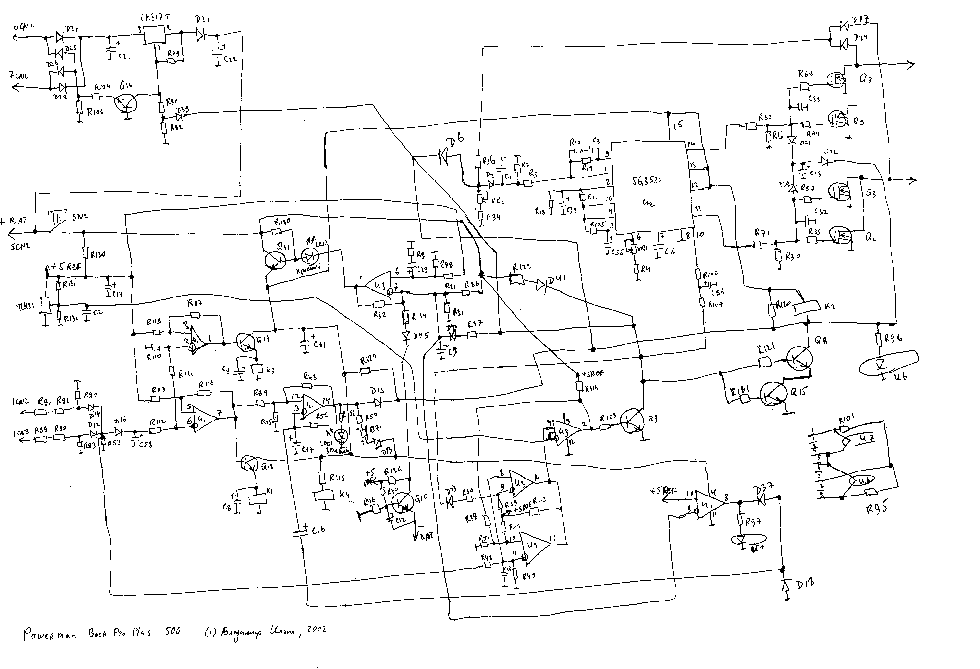
PowerMan UPS/Inverters manufactures uninterruptible power supplies and voltage regulators. The business was founded in 1993 and was involved in distribution prior to the year 2000. PowerMan specializes in providing reliable power solutions, including uninterruptible power supplies (UPS) and voltage regulators,...
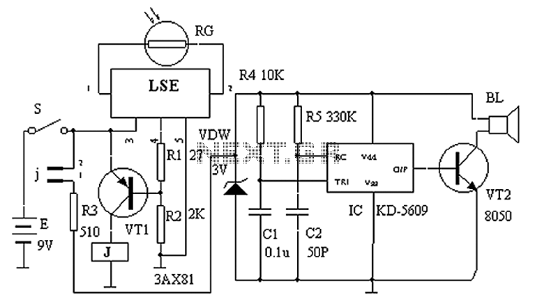
The circuit principle is illustrated in the accompanying figure. When the night light shines on the photosensitive resistor RG, it exhibits a high resistance (significantly greater than 50K). As a result, the output of the LSE pin is low,...
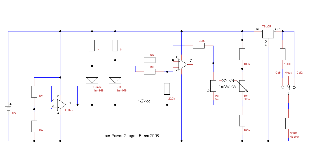
For some time, a method to measure laser power has been sought without incurring significant expenses on a power meter. Initially, constructing such a device may seem unfeasible. To create a cost-effective laser power measurement system, one approach involves utilizing...