
10 Bit A-D converter circuit

The described circuit operates as a precise analog-to-digital converter (ADC) using the LT1016 operational amplifier. The system initiates a conversion process when a control pulse is applied, triggering Q1 to reset the capacitor. The 1000 pF capacitor's rapid discharge and subsequent linear charging behavior are critical for generating a stable ramp voltage. The ramp voltage, reaching 2.5 V over 10 microseconds, serves as the reference signal for the LT1016, which functions as a comparator.
The comparator's role is to assess the relationship between the ramp voltage (Ex) and the unknown voltage applied to its negative input. The choice of resistor values (2.5 kΩ and 7.5 kΩ) determines the scaling of the input voltage range. For lower voltage ranges (0 V to 2.5 V), the 2.5 kΩ resistor allows for a direct comparison, while the grounded 2.5 kΩ resistor in the higher range (0 V to 10 V) adjusts the input sensitivity accordingly.
The output pulse width generated by the LT1016 is a critical parameter for subsequent digital processing. This pulse width, which varies with the input voltage Ex, is used to gate a high-frequency clock signal of 100 MHz. The resulting clock pulses are quantized into 1024 discrete levels, providing a high-resolution output suitable for digital applications. The relationship between the output pulses and the input voltage allows for accurate representation and processing of analog signals in digital systems, making this circuit highly effective for applications requiring precise voltage measurements and conversions.Each time a pulse is applied to the conversion of the control input, Ql resets the 1000 pF capacitor to 0 V. This action takes 200 ns to reset the falling edge of the convert command pulse, the capacitor begins to charge linearly.
In exactly 10 microseconds, it loads to 2.5 V. The ramp is 10 microseconds applied to the positive input of the LTl016. The LT1016 compares the ramp Ex, the unknown, its negative input. For a 0 V - 2.5 V range, Ex is applied to the resistance of 2.5 k ohm. On a 0 V - 10 V, 2.5 k ohm resistor is grounded, and Ex is applied to the resistance of 7.5 k ohm. LT1016 output is a pulse whose width is directly dependent on the value of Ex. This pulse width is used at the gate a clock at 100 MHz. The 100 MHz clock pulse bursts that appear at the output is proportional to Eg for a 0 V - 10 V input, 1024 pulses appear full scale from 512 to 5.00 V, etc. 🔗 External reference
Related Circuits
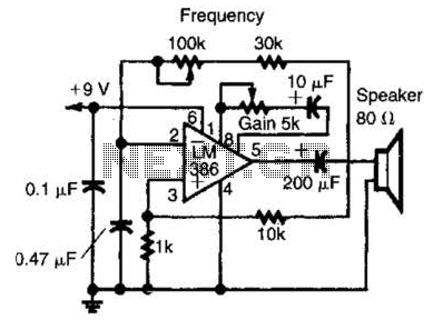
An LM386 audio power IC is configured as a feedback oscillator. It can operate with a supply voltage ranging from 6 to 12 V. The circuit is capable of driving a loudspeaker. The LM386 is a low-voltage audio power amplifier...
This circuit is a constant current protection type that limits the output current to a specific value in cases of over-current and short-circuit conditions. When the output current exceeds this limit, the output voltage decreases. The CW200 power management...
The development of the entire system necessitated a thorough identification of all processes related to the laser controller. The initial diagram outlines the primary physical components utilized in the CNC laser system. The setup includes a power supply, a...
Direct distribution lightning generator with a capacity range of 300 to 1500 kW, designed for single-phase applications. The generator facilitates the direct distribution of electrical energy, providing reliable performance for various applications. The lightning generator operates within a specified power...
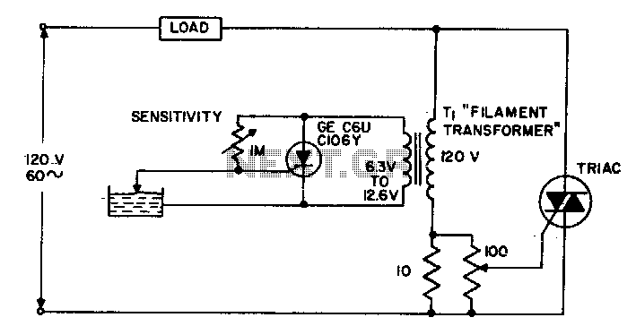
The circuit supplies power to the load until water conducts through the probe, allowing gate current to bypass from the low current SCR. This configuration provides an isolated low voltage probe to meet safety requirements. The described circuit operates as...
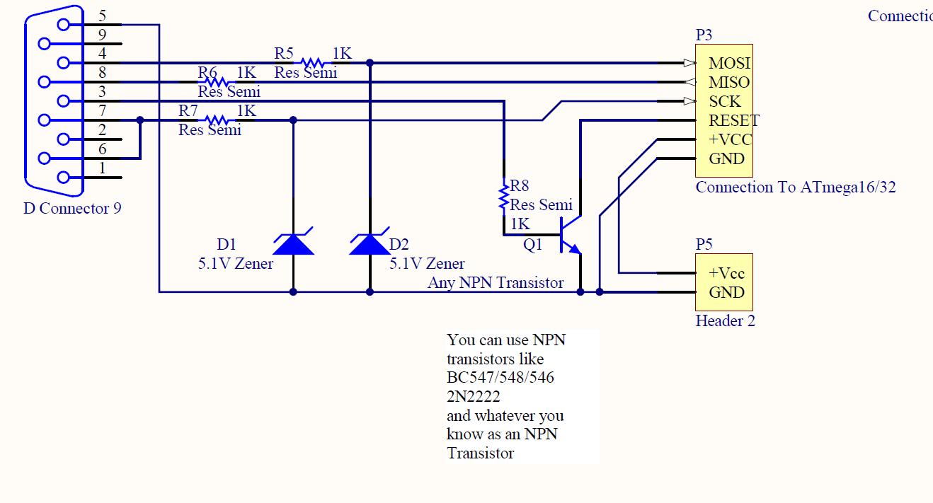
ISP programmer with circuit diagram for AVR Atmega32 microcontroller. This ISP burner circuit is an adaptation of the Pony programmer and uses PonyProg software. The ISP (In-System Programming) programmer designed for the AVR Atmega32 microcontroller facilitates the programming of the...
Warning: include(partials/cookie-banner.php): Failed to open stream: Permission denied in /var/www/html/nextgr/view-circuit.php on line 713
Warning: include(): Failed opening 'partials/cookie-banner.php' for inclusion (include_path='.:/usr/share/php') in /var/www/html/nextgr/view-circuit.php on line 713