
100Khz-multiple-output-switching-power-supply
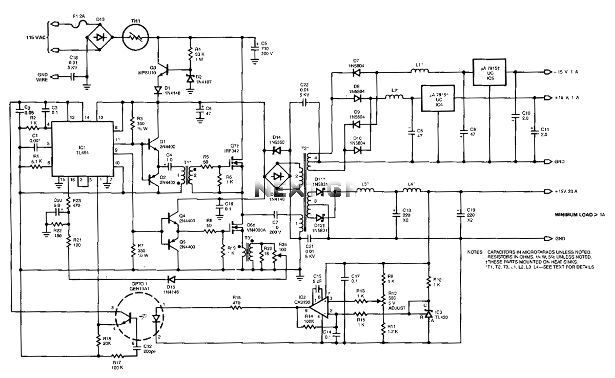
The power supply employs two VN4000A 400-V MOSPOWER FETs configured in a half-bridge arrangement. It provides outputs of +5 V at 20 A and ±15 V (or ±12 V) at 1 A. The low-current outputs utilize linear three-terminal regulators, allowing for either ±12 V or ±15 V to be achieved with a straightforward modification to the transformer’s secondary windings. A TU94 switching regulator integrated circuit delivers pulse-width modulation control and drive signals for the power supply. The upper MOSPOWER FET, designated as Q7, in the power switch stage is activated by a basic transformer drive circuit. The lower MOSFET, Q6, is ground-referenced and is directly driven from the control integrated circuit.
The power supply circuit utilizes a half-bridge topology, which is advantageous for its efficiency and ability to provide high voltage outputs. The VN4000A MOSFETs are selected for their high voltage rating, enabling the circuit to handle voltages up to 400 V, making them suitable for various applications that require robust power handling.
The output specifications include a regulated +5 V output capable of delivering up to 20 A, which is significant for powering high-current devices. The ±15 V and ±12 V outputs at 1 A are typically used in analog circuitry where dual supply voltages are necessary for operational amplifiers and other analog devices. The use of linear three-terminal regulators for these outputs helps maintain a stable voltage, but it is essential to consider the thermal performance and heat dissipation requirements, especially at higher loads.
The TU94 switching regulator IC is a crucial component that provides pulse-width modulation (PWM) control, which is essential for regulating the output voltage efficiently. This method of control allows for reduced power loss compared to linear regulation, particularly in high-power applications. The transformer drive circuit for the upper MOSFET (Q7) ensures that the switching frequency is maintained, which is important for the overall performance of the power supply.
The direct drive of the lower MOSFET (Q6) from the control IC simplifies the circuit design and improves response times, as it eliminates the need for additional components that could introduce delays or complexity. The ground-referenced configuration of Q6 further enhances stability and reliability in operation.
Overall, this power supply design effectively combines high-efficiency switching technology with reliable linear regulation to deliver versatile output options suitable for a range of electronic applications.The power supply uses two VN4000A 400-V MOSPOWER FETs in a half-bridge power switch configuration. Outputs available are + 5 Vat 20 A and ±15 V (or ±12 V) at 1 A. Since linear three-terminal regulators are used for the low-current outputs, either ±12 V or ±15 V can be made available with a simple change in the transformer secondary windings. A TU94 switching regulator IC proVides pulse-width modulation control and drive signals for the power supply.
The upper MOSPOWER FET, Q7. in the power switch stage is driven by a simple transformer drive circuit. The lower MOS. Q6, since it is ground referenced. is directly driven from the control !C. 🔗 External reference