
100M-baud-fiber-optic-receiver
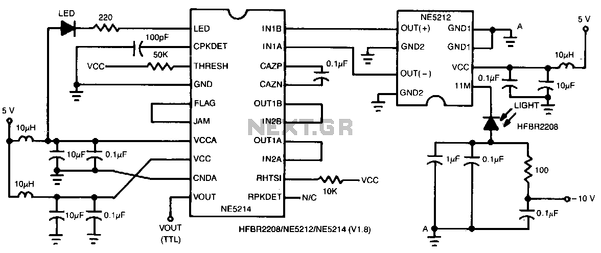
This two-chip receiver, designed for low-cost fiber optic applications at 100-M baud (50 MHz), features a minimal external component count. The receiver consists of pre-amplifier and post-amplifier integrated circuits (ICs) for enhanced stability. The preamplifier IC is characterized by low noise and a differential transresistance design. The postamplifier IC includes an auto-zeroed first stage with noise shaping, a high-gain symmetrical-limiting amplifier, and a TTL output buffer with matched rise and fall times. A wide-band full-wave rectifier serves as a link-status indicator. To ensure stability, a surface mount, small outline (SO) package is utilized. The received signal, ranging from -35 dBm optical (average) to -9 dBm, is converted into a small unipolar current by the pin diode, which then feeds its signal current to a preamplifier, such as the NE5212. The output from the preamplifier is directed to a high-gain limiting amplifier, commonly referred to as the post amp. The NE5214/NE5217 postamplifiers are economical ICs that provide up to 60 dB of gain at 50 MHz, elevating millivolt level signals to TTL levels. The postamplifier IC features an auto-zeroed first stage with noise shaping, a high-gain symmetrical-limiting amplifier, and a TTL output buffer with matched rise and fall times. A secondary amplifier chain operates as a link-status indicator.
The electronic schematic for this two-chip receiver is designed to optimize performance for fiber optic applications. The preamplifier stage, utilizing the NE5212, is critical for amplifying weak optical signals received from the pin diode. This diode is responsible for converting the optical signal into a small unipolar current, which is essential for further amplification. The differential transresistance design of the preamplifier minimizes noise, thereby enhancing the signal-to-noise ratio, which is crucial for maintaining signal integrity at high baud rates.
Following the preamplifier, the signal is processed by the postamplifier stage, which can be implemented using NE5214 or NE5217 ICs. These components are designed to deliver high gain, enabling the circuit to amplify signals from millivolt levels to TTL levels effectively. The incorporation of noise shaping in the auto-zeroed first stage of the postamplifier contributes to further reduction of unwanted noise, ensuring that the output signal remains clean and stable.
The high-gain symmetrical-limiting amplifier within the postamplifier is engineered to provide consistent output levels, regardless of variations in input signal strength. This characteristic is particularly beneficial in fiber optic communications, where signal levels can fluctuate due to various factors, including distance and attenuation. The matched rise and fall time TTL output buffer ensures that the output signal is compatible with standard digital logic levels, facilitating easy integration with subsequent digital processing stages.
The overall architecture of the receiver, including the use of a wide-band full-wave rectifier as a link-status indicator, adds a layer of functionality by allowing users to monitor the operational status of the fiber optic link. This feature is vital for maintenance and troubleshooting purposes, ensuring that any issues with signal transmission can be promptly identified and addressed. The compact design, achieved through the use of surface mount technology, not only reduces the footprint of the circuit but also enhances reliability by minimizing the number of external components required.This two-chip receiver with minimum external component count has been designed for low-cost fiber optic applications to 100-M baud (50 MHz). The receiver is divided into pre-and postamplifier !Cs for increased stability. The preamplifier IC features low noise with a differential transresistance design. The postamplifier IC incorporates an auto-zeroed first stage with noise shaping, high-gain symmetrical-limiting amplifier, and a matched rise/fall time TTL output buffer.
-A wide-band full-wave rectifier functions as a link-status indicator. To ensure stability, a surface mount, small outline (SO), package is used. The received signal in the -35 dBm optical (average) to -9 dBm range is converted into a small unipolar current by the pin diode. The pin diode then feeds its signal current to a preamplifier, such as the NE5212. The preamplifier output is fed to a high-gain limiting amplifier, simply known as the post amp. The NE5214/NE5217 postamplifiers are low-cost !Cs that provide up to 60 dB of gain at 50 MHz to bring mV level signals up to TTL levels.
The postamplifier IC incorporates an auto-zeroed first stage with noise shaping, a high-gain symmetrical-limiting amplifier, and a matched rise/fall time TTL output buffer. A secondary amplifier chain functions as a link-status indicator. 🔗 External reference