1296Mhz-solid-state-power-amplifier

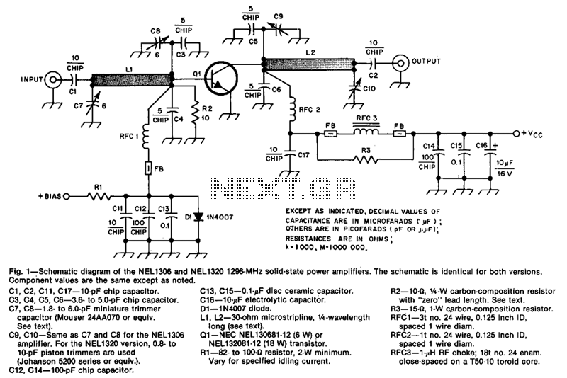
The design incorporates 30-ohm, 1/4 microstrip lines on the input and output. Capacitors C3, C4, C7, and C8, along with inductor L1, form a pi network that matches the low input impedance of the device to 50 ohms. Capacitors C5, C6, C9, C10, and the 30-ohm transmission line L2 create an output pi network that maximizes power transfer to 50 ohms. Capacitor C10 is not always necessary, depending on variations among devices and circuit board material. Bias is provided by resistors R1, R2, and diode D1. Resistor R1 can be optimized, if desired, to adjust the collector idling current.
The circuit design utilizes microstrip lines, specifically configured to operate at a characteristic impedance of 30 ohms on both the input and output paths. These microstrip lines are essential for maintaining signal integrity and minimizing reflections in RF applications. The pi network formed by capacitors C3, C4, C7, and C8, in conjunction with inductor L1, is crucial for impedance matching. This arrangement ensures that the low input impedance of the device is effectively matched to the standard 50-ohm system, facilitating optimal power transfer and minimizing signal loss.
On the output side, the inclusion of capacitors C5, C6, C9, C10, and transmission line L2 creates another pi network that is designed to maximize the power transfer efficiency to a 50-ohm load. The presence of capacitor C10 is conditional; its necessity may vary based on the specific characteristics of the devices and the materials used in the circuit board, which can affect the overall performance of the network.
Biasing of the circuit is accomplished through the use of resistors R1 and R2, along with diode D1, which together provide the necessary operating conditions for the active device. Resistor R1 can be fine-tuned to optimize the collector idling current, allowing for adjustments that can enhance the performance of the circuit under varying operational conditions. This flexibility in biasing is critical in applications where precise control over the device's operating point is required. Overall, the design emphasizes efficient signal management and adaptability to various device specifications and circuit board materials.The design incorporates 30-0, 1/4;.. microstrip lines on the input and output. C3, C4, C7, and C8, along with Ll, form a pi network that matches the low-input impedance of the device to 50 0. C5, C6, C9, ClO, and 30-0 transmission line L2 form an output pi network that maximizes power transfer to 50 0.
ClO is not always necessary, depending on variations among devices and circuitboard material. Bias is provided by Rl, R2, and Dl. Rl can be optimized, if desired, to adjust the collector idling current. 🔗 External reference