
+15-V-1-a-regulated-power-supply
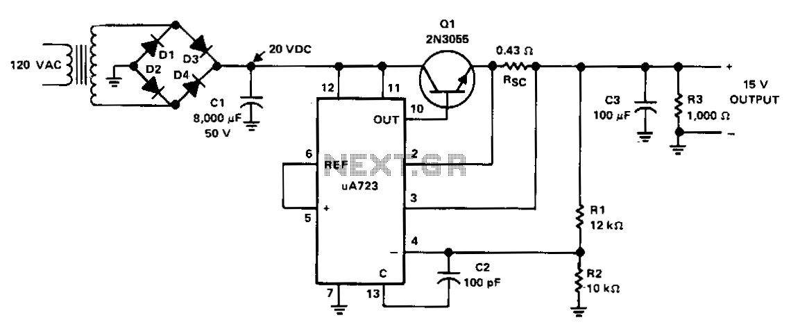
The power supply receives +20 VDC from the rectifier/filter section. This voltage is applied to pins 11 and 12 of the uA723 voltage regulator, as well as to the collector of the 2N3055 series-pass transistor. The output voltage is sampled through resistors R1 and R2, yielding approximately 7 V with respect to ground at pin 4. The reference terminal at pin 6 is connected directly to pin 5, which is the non-inverting input of the error amplifier. For precise adjustment of the output voltage, a potentiometer can be placed between R1 and R2. A 100-pF capacitor is connected from pin 13 to pin 4 to provide gain compensation for the amplifier.
The base drive to the 2N3055 pass transistor is supplied by pin 10 of the uA723. The desired output of the supply is limited to a maximum of 1 A, with the current limit set to 1.5 A using a sense resistor (Rsc) valued at 0.433 ohms. A 100 µF electrolytic capacitor is employed for reducing ripple voltage at the output. An output resistor provides stability for the power supply under no-load conditions. The 2N3055 pass transistor must be mounted on an appropriate heatsink to ensure efficient thermal management.
The described power supply circuit utilizes the uA723 voltage regulator to provide a stable output voltage with adjustable characteristics. The input voltage of +20 VDC is crucial for the operation of the regulator, enabling it to maintain the desired output voltage despite variations in load conditions. The configuration of R1 and R2 allows the output voltage to be sampled and compared against a reference voltage, enabling the error amplifier to adjust the base drive to the 2N3055 transistor accordingly.
The inclusion of a potentiometer between R1 and R2 facilitates fine-tuning of the output voltage, allowing for precise calibration based on specific application requirements. The gain compensation capacitor (100 pF) enhances the stability of the amplifier, ensuring that the system responds adequately to transient load changes without oscillation.
The current limiting feature implemented via the sense resistor (Rsc) is essential for protecting the circuit from excessive current draw, which could lead to overheating or damage. The choice of a 100 µF electrolytic capacitor at the output is significant in reducing ripple voltage, thus improving the quality of the power supply output. The output resistor plays a critical role in maintaining stability, especially in scenarios where the power supply is operating without a load.
Finally, the thermal management of the 2N3055 pass transistor is crucial, as it is responsible for regulating the output voltage and can generate substantial heat during operation. Proper heatsinking is necessary to maintain the transistor within its safe operating temperature range, ensuring reliable performance of the power supply circuit over extended periods.The supply receives + 20 Vdc from the rectifier/filter section. This is applied to pins 11 and 12 of the uA723, as well as to the collector of the 2N3055 series-pass transistor. The output voltage is sampled through R1 and R2, providing about 7 V with respect to ground at pin 4.
The reference terminal at pin 6 is tied directly to pin 5, the noninverting input of the error amplifier. For fine trimming the output voltage, a potentiometer can be installed between R1 and R2. A 100-pF capacitor from pin 13 to pin 4 furnishes gain compensation for the amplifier. Base drive to the 2N3055 pass transistoris furnished by pin 10 of the uA 723. Since the desired output of the supply is 1 A. maximum current limit is set to 1.5 A by resistor Rsc whose value is 0.433 0. A 100-J🔗 External reference
The base drive to the 2N3055 pass transistor is supplied by pin 10 of the uA723. The desired output of the supply is limited to a maximum of 1 A, with the current limit set to 1.5 A using a sense resistor (Rsc) valued at 0.433 ohms. A 100 µF electrolytic capacitor is employed for reducing ripple voltage at the output. An output resistor provides stability for the power supply under no-load conditions. The 2N3055 pass transistor must be mounted on an appropriate heatsink to ensure efficient thermal management.
The described power supply circuit utilizes the uA723 voltage regulator to provide a stable output voltage with adjustable characteristics. The input voltage of +20 VDC is crucial for the operation of the regulator, enabling it to maintain the desired output voltage despite variations in load conditions. The configuration of R1 and R2 allows the output voltage to be sampled and compared against a reference voltage, enabling the error amplifier to adjust the base drive to the 2N3055 transistor accordingly.
The inclusion of a potentiometer between R1 and R2 facilitates fine-tuning of the output voltage, allowing for precise calibration based on specific application requirements. The gain compensation capacitor (100 pF) enhances the stability of the amplifier, ensuring that the system responds adequately to transient load changes without oscillation.
The current limiting feature implemented via the sense resistor (Rsc) is essential for protecting the circuit from excessive current draw, which could lead to overheating or damage. The choice of a 100 µF electrolytic capacitor at the output is significant in reducing ripple voltage, thus improving the quality of the power supply output. The output resistor plays a critical role in maintaining stability, especially in scenarios where the power supply is operating without a load.
Finally, the thermal management of the 2N3055 pass transistor is crucial, as it is responsible for regulating the output voltage and can generate substantial heat during operation. Proper heatsinking is necessary to maintain the transistor within its safe operating temperature range, ensuring reliable performance of the power supply circuit over extended periods.The supply receives + 20 Vdc from the rectifier/filter section. This is applied to pins 11 and 12 of the uA723, as well as to the collector of the 2N3055 series-pass transistor. The output voltage is sampled through R1 and R2, providing about 7 V with respect to ground at pin 4.
The reference terminal at pin 6 is tied directly to pin 5, the noninverting input of the error amplifier. For fine trimming the output voltage, a potentiometer can be installed between R1 and R2. A 100-pF capacitor from pin 13 to pin 4 furnishes gain compensation for the amplifier. Base drive to the 2N3055 pass transistoris furnished by pin 10 of the uA 723. Since the desired output of the supply is 1 A. maximum current limit is set to 1.5 A by resistor Rsc whose value is 0.433 0. A 100-J
Warning: include(partials/cookie-banner.php): Failed to open stream: Permission denied in /var/www/html/nextgr/view-circuit.php on line 713
Warning: include(): Failed opening 'partials/cookie-banner.php' for inclusion (include_path='.:/usr/share/php') in /var/www/html/nextgr/view-circuit.php on line 713