
250mW audio Amplifier

R1 = 4.7 kOhm
R2 = 82 kOhm
R3 = 12 kOhm
R4 = 1.8 kOhm
P1 = 10 kOhm
C1 = 10 V ?F/10
C2 = 100 V ?F/10
C3 = 220 V ?F/10
D1, D2 = 1N4148
T1 = 547 BC
T2 = 337 BC
T3 = 327 BC
The described circuit functions as a small booster amplifier, utilizing a balanced amplifier stage to achieve its purpose. The design incorporates a quiescent current setting mechanism through the use of diodes D1 and D2, specifically 1N4148, which are pivotal in maintaining stable operating conditions. The quiescent current is temperature-dependent, which can lead to performance variations if transistors T2 and T3 operate at significantly higher temperatures compared to the diodes. This temperature sensitivity necessitates careful thermal management, making it advisable to mount the transistors on a small aluminum plate to enhance heat dissipation. The use of super glue for this mounting ensures a secure thermal connection.
The circuit operates with a supply voltage of 9 volts, which is suitable for the selected components. The resistors (R1, R2, R3, R4, and P1) are strategically chosen to set the biasing conditions and gain of the amplifier. R1 (4.7 kOhm) and R2 (82 kOhm) likely form part of the feedback network, while R3 (12 kOhm) and R4 (1.8 kOhm) help in establishing the input and output impedance levels, optimizing the amplifier's performance.
Capacitors C1 (10 V, ?F), C2 (100 V, ?F), and C3 (220 V, ?F) are included in the design to filter noise and stabilize the power supply, ensuring that the amplifier operates efficiently by smoothing out voltage fluctuations. Transistors T1 (BC547), T2 (BC337), and T3 (BC327) are utilized to provide the necessary amplification, with T1 likely serving as the input stage and T2 and T3 configured for output stage amplification. This arrangement enables the circuit to effectively boost low-level signals to a higher output level, suitable for driving subsequent stages or loads.
Overall, this circuit design exemplifies a straightforward yet effective approach to creating a small booster amplifier with considerations for thermal management, component selection, and signal integrity.This design can be used as a small booster. The amplifier is built around a balance stage. The quiescent current is set by diodes D1 and D2. The simplicity of the circuit, the quiescent current depends on the temperature of the diodes. When T2 and T3 have a much higher temperature than the diodes, can be annoying. The transistors is a cooling solution. It is best the two transistors on a small aluminum plate with some super glue to glue. The supply voltage is 9 volts. Parts List R1 = 4.7 kOhm R2 = 82 kOhm R3 = 12 kOhm R4 = 1.8 kOhm P1 = 10 kOhm C1 = 10 V ?F/10 C2 = 100 V ?F/10 C3 = 220 V ?F/10 D1, D2 = 1N4148 T1 = 547 BC T2 = 337 BC T3 = 327 BC 🔗 External reference
Related Circuits
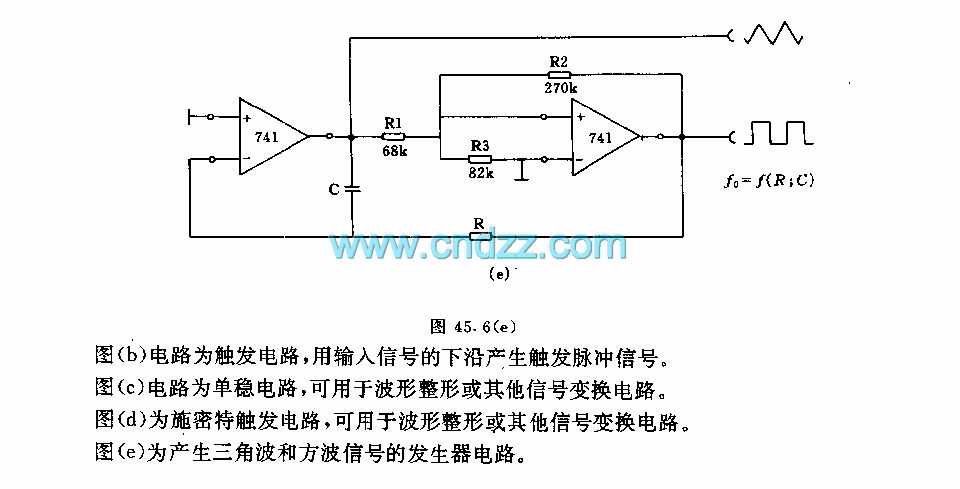
Figure a illustrates a multivibrator circuit capable of generating a square wave signal. Figure b depicts a flip-flop circuit that utilizes the falling edge of the input signal to produce a trigger pulse signal. Figure c represents a monostable...
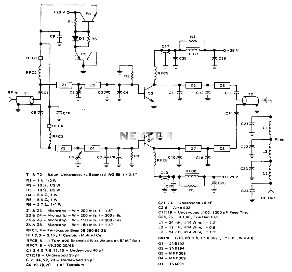
This 100-watt linear amplifier can be built using two MRF309 transistors in a push-pull configuration, requiring only 16 watts of drive power within the frequency range of 420 to 450 MHz. It operates from a 28-volt supply and achieves...
Can be directly connected to CD players, tuners and tape recorders. Tested with several headphone models of different impedance: 32, 100, 245, 300, 600 & 2000 Ohms. Schematic shows left channel only. B1, SW1, J1 & C3 are common...
This is an economical 150 Watt amplifier circuit that utilizes two complementary Darlington power transistors, TIP 142 and TIP 147. It is capable of delivering a robust 150 W RMS to a 4 Ohm speaker, offering significant audio output....

The circuit presented is a three-input microphone mixer and preamplifier utilizing the LM348 integrated circuit. The LM348 is a high-gain, internally compensated quad operational amplifier featuring a class AB output stage. It has a very low input supply current...
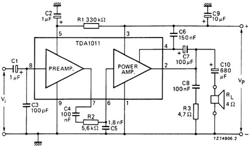
The following schematic illustrates the design of a 4 Watt Amplifier Circuit Diagram intended for portable radio applications, utilizing the TDA1011 integrated circuit from Philips Semiconductor. The 4 Watt Amplifier Circuit is designed to provide audio amplification in portable radio...
Warning: include(partials/cookie-banner.php): Failed to open stream: Permission denied in /var/www/html/nextgr/view-circuit.php on line 713
Warning: include(): Failed opening 'partials/cookie-banner.php' for inclusion (include_path='.:/usr/share/php') in /var/www/html/nextgr/view-circuit.php on line 713