
300V-pulse-generator
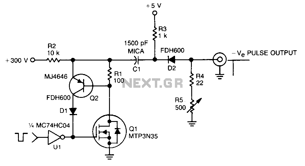
In this TMOS pulser, a negative-going pulse is applied to U1, a high-speed CMOS buffer, which directly drives the gate of Q1, an MTP3N35. If only a 100-V pulse is required, the MTA6N10 can be used. The pulse output across R2 is differentiated by R3/C1 and appears as a negative-going spike at the output terminal.
The TMOS pulser circuit operates by utilizing a high-speed CMOS buffer (U1) to generate a negative-going pulse that controls the gate of a TMOS transistor (Q1). The MTP3N35 is selected for applications requiring higher voltage handling, while the MTA6N10 can be employed for applications limited to 100 volts.
In this configuration, the pulse is applied to the gate of Q1, allowing it to switch on and off rapidly, thereby controlling the output signal. The output signal is taken across resistor R2. To shape this output signal into a desired waveform, a differentiating circuit is formed by the combination of resistor R3 and capacitor C1. This differentiation process converts the square wave pulse into a negative-going spike, which is the desired output waveform at the terminal.
The choice of components, including the values for R2, R3, and C1, will significantly affect the characteristics of the output spike, such as its amplitude and duration. Proper selection and tuning of these components are crucial for achieving optimal performance in applications that require precise timing and control of the output pulse characteristics.In this TMOS pulser, a negative-going pulse is applied to Ul, a high-speed CMOS buffer, which directly drives the gate ofQl, an MTP3N35. If only a 100-V pulse is required, the MTA6Nl0 can be used. The pulse output across R2 is differentiated by R3/Cl and appears as a negative-going spike at the output terminal. 🔗 External reference