
3GPP FDD User Equipment Receiver Test

The 3GPPFDD_UE_RX test bench serves as a critical tool in the evaluation of 3GPP FDD user equipment receivers, ensuring compliance with industry standards and facilitating the analysis of various performance metrics. By providing a structured approach to testing, the bench allows engineers to assess the efficacy of RF devices under real-world conditions, thereby contributing to the advancement of telecommunications technology. The integration of advanced simulation techniques, such as co-simulation between different modeling environments, further enhances the accuracy and reliability of the test results. This comprehensive testing framework is essential for the development and optimization of next-generation wireless communication systems.3GPPFDD_UE_RX is the test bench for 3GPP FDD user equipment receiver testing. The test bench provides a way for users to connect to an RF circuit device under test and determine its performance using pre-defined test bench measurements. This test bench provides signal measurements for reference sensitivity level, maximum input level, adjacent chan
nel selectivity, and blocking and intermodulation characteristics. The signal and the measurements are designed according to 3GPP Technical Specifications TS 25. 101 and TS 34. 121. Versions supported are 2000-03, 2000-12, and 2002-03. This 3GPP FDD signal model is compatible with Agilent E4438C ESG Vector Signal Generator, Option 400 (3GPP W-CDMA Firmware Option for the E4438C ESG Vector Signal Generator). Details regarding Agilent E4438C ESG are included at the website. This test bench includes a TX DSP section, an RF modulator, RF output source resistance, an RF DUT connection, RF receivers, and DSP measurement blocks as illustrated in the following figure.
The generated test signal is sent to the DUT. The 3GPPFDD_UE_RX test bench uses the downlink 12. 2kbps reference measurement channel. One 12. 2kbps DTCH (dedicated transport channel) and one 2. 4kbps DCCH (dedicated control channel) are multiplexed into one 60kbps DPCH (dedicated physical data channel). The signal source includes one DPCH, one PCCPCH (primary common control physical channel), one PSCH (primary synchronization channel), one SSCH (secondary synchronization channel), one CPICH (common pilot channel), and one PICH (page indication channel).
For the maximum input level measurement, the OCNS interference is set to the power necessary to achieve the required DPCH_Ec/I or of -19dB. The gain of the other channels remain the same. An example design using this template is available; from the ADS Main window click File > Example Project > WCDMA3G_RF_Verification_prj > 3GPPFDD_UE_RX_test.
dsn. The following sections provide details for setting up a test bench, setting measurement parameters for more control of the test bench, simulation measurement displays, and baseline performance. Cosimulation occurs between the test bench (using Agilent Ptolemy Data Flow simulation technology) and the DUT (using Agilent Circuit Envelope simulation technology).
Each technology requires its own simulation time step with time-step coordination occurring in the interface between the technologies. CE_TimeStep defines the Circuit Envelope simulation time step to be used with this DUT. The CE_TimeStep must be set to a value equal to or a submultiple of (less than) WTB_TimeStep; otherwise, simulation will stop and an error message will be displayed.
The CE_TimeStep value is exported to the Choosing Analyses window in the Circuit Envelope Time Step field when the user clicks OK in the Wireless Test Bench Setup window. Note that WTB_TimeStep is not user-settable. Its value is derived from other test bench parameter values; with default settings WTB_TimeStep=1/(3.
84e6G—8) sec. The value is displayed in the Data Display pages as TimeStep. More control of the test bench can be achieved by setting Basic Parameters, Signal Parameters, and parameters for each measurement. For details refer to Parameter Settings. The RF modulator (shown in the block diagram in Receiver Wireless Test Bench Block Diagram ) uses FSource, SourcePower ( Required Parameters ), MirrorSourceSpectrum ( Basic Parameters), GainImbalance, PhaseImbalance, I OriginOffset, Q OriginOffset, and IQ Rotation ( Signal Parameters ).
The RF output resistance uses SourceR, SourceTemp, and EnableSourceNoise ( Basic Parameters ). The RF output signal source has a 50-ohm (default) output resistance defined by SourceR. RF output (and input to the RF DUT) is at the frequency specified (FSource), with the specified source resistance (SourceR) and with power (SourcePower) delivered into a matched load of resistance SourceR. The RF signal has additive Gaussian noise power set by resistor temperature (SourceTemp) (when EnableSourceNoise=YES).
More control of the Circuit Envelope simulation of the RF DUT is achieved by selecting Options in the Choosing Analysis window. These advanced options include enabling Automatic Behavioral Modeling (which may speed up the RF DUT simulation by over 10X), and setting Circuit Envelope parameters.
Setting these simulations options is described in Setting Automatic Behavioral Modeling Parameters and Setting Circuit Envelope Analysis Parameters in the Wireless Test Bench Simulation documentation. Simulation results will appear in a Data Display window for each measurement. Simulation Measurement Displays describes results for each measurement available for this test bench.
🔗 External reference
Related Circuits
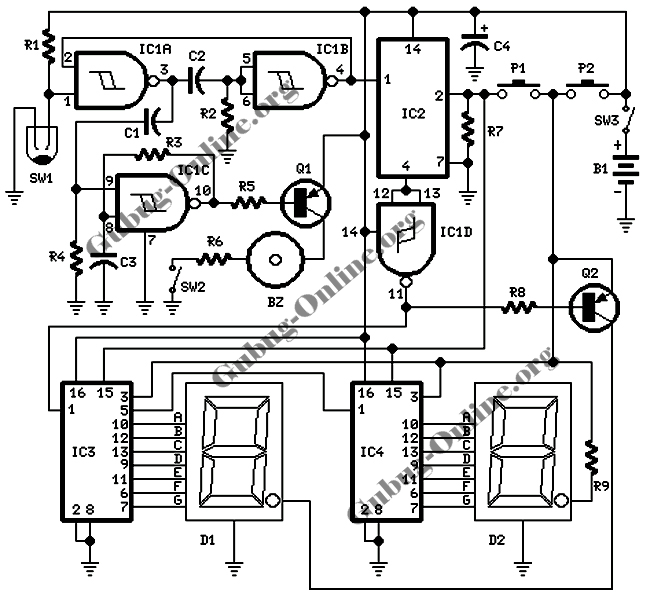
This design features a signal logic tester that utilizes a common cathode seven-segment display. The display indicates a logic level "1" (represented by an "H" on the display) or a logic level "0" (represented by an "L" on the...
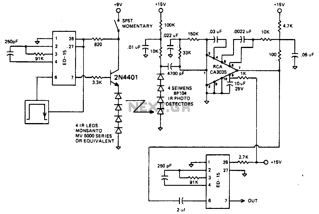
The circuit is designed to operate at 25 kHz. The data stream controls the 2N4401 transistor, turning it fully on or off based on the coded state. This action switches the series of infrared LEDs on and off. The...

The barrier measurement method for distance is based on assessing the strength of a bound signal. A reflection wave is captured with an acceptor transducer, which emits a sine wave signal. The amplitude of this signal varies with the...
To build a Spectrum analyzer I needed a tuner. I also needed to learn how to control the tuner. In some old broken TV I found the tuner UV916. It is a common used tuner. The tuner is PLL...
The regen is basically an oscillator circuit with a gain control that allows the user to adjust the feedback to a point just below oscillation or, quite often, just above the critical level such that a small oscillation is...
This technical note focuses on determining the system specifications of a CDMA receiver to establish practical specifications for a low noise amplifier and down converter. The design of a CDMA (Code Division Multiple Access) receiver necessitates a comprehensive understanding of...