
+5V, 1A DC output flyback switching power supply circuit TOP100Y
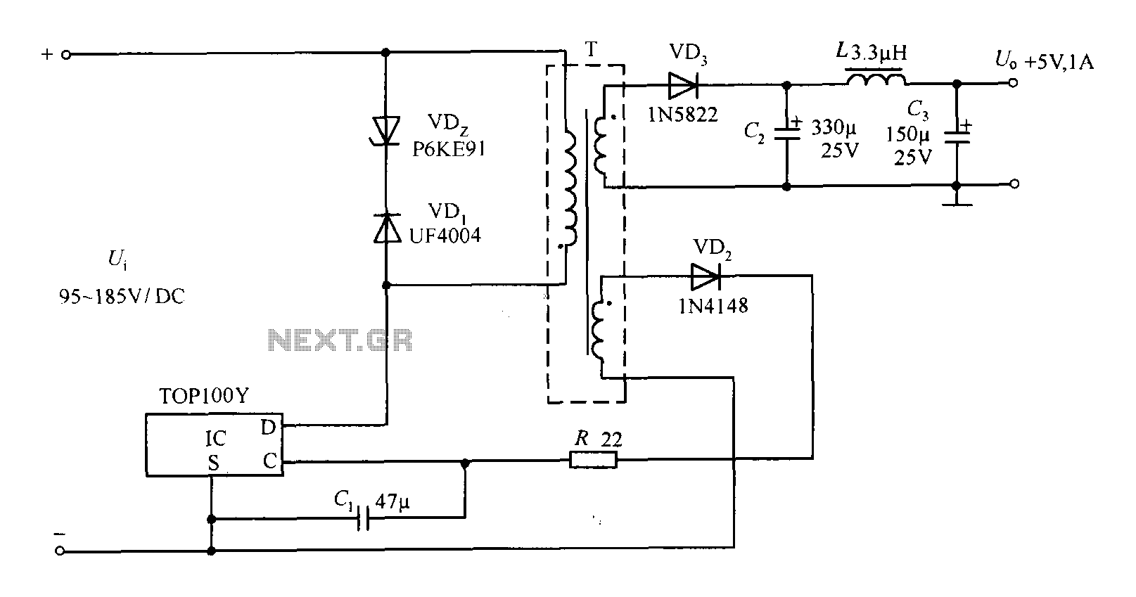
The TOP100Y flyback DC switching power supply circuit is designed to convert a high-voltage DC input into a stable low-voltage output, specifically +5V at 1A. This design is particularly advantageous in applications where electrical isolation is necessary, such as in sensitive electronic devices that may be adversely affected by voltage fluctuations or noise on the input supply.
The feedback mechanism is crucial for maintaining output stability. The feedback circuit monitors the output voltage and adjusts the switching operation of the power supply to ensure that the output remains within specified limits, even as the load conditions change. The voltage regulation of 1.25% indicates a high level of precision, ensuring that the output voltage remains stable across a wide range of input voltages and load currents.
The load regulation of 4.5% signifies that the output voltage will vary slightly with changes in load current, but this variation is kept within acceptable limits for most applications. The output ripple voltage of 25mV indicates that the power supply produces a clean DC output with minimal fluctuations, which is essential for powering sensitive electronics.
The switching frequency of 100kHz is typical for flyback converters, allowing for efficient energy transfer while minimizing losses. The use of transient voltage suppression diodes (VDz, P6KE91) in the clamp circuit protects the power supply from voltage spikes, while the ultra-fast recovery diode (VDl, UF4004) ensures quick response times during switching transitions, further contributing to the overall efficiency and reliability of the circuit.
The rectification and filtering stage, which includes components VD3, C2, L, and C3, plays a vital role in converting the high-frequency AC output from the transformer into a smooth DC voltage. The feedback loop, which incorporates the feedback coil voltage, resistor R, and capacitor C1, is designed to stabilize the control terminal of the TOP100Y. The dual function of capacitor C1 as a control loop compensation capacitor allows for tuning the response of the feedback loop, which is critical for maintaining stable operation and preventing oscillations.
Overall, the TOP100Y flyback DC switching power supply circuit exemplifies a well-engineered solution for converting and regulating DC power, suitable for various applications requiring reliable and isolated power sources.TOP100Y constituted by a + 5v, 1A output flyback DC switching power supply circuit is shown. This flyback switching power supply output voltage is directly regulated by a feedback circuit for applications requiring isolation and load change is small. When the DC input voltage Ui = 95 ~ 185V, the voltage regulation Sv = 1.25%. When the load current changes from l0% to l00%, the load regulation SI = 4.5%. The output ripple voltage is 25mV. Switching frequency is still 100kHz (typ).Clamp circuit consists of transient voltage suppression diodes VDz (P6KE91) and ultra-fast recovery diode VDl (UF4004) components.
Secondary voltage VD3, C2, L, C3 after rectifier filter to obtain a + 5V output. After the adoption of the feedback coil voltage VD2, R and Cl rectifier filter, applied to the control terminal of TOPl00Y. Cl doubles as a control loop compensation capacitor, and decided to auto-restart frequency.
Related Circuits
LEDs are rated for a continuous current of only 30 mA, while this circuit operates them at approximately 50 mA. Although this is acceptable for low duty cycles with short pulses, the intended design has a high duty cycle....
The mixer circuit features two line inputs and two microphone inputs, along with two line outputs. The microphone inputs are designed for low-impedance dynamic microphones with an impedance range of 200-1000 ohms. This simple mixer was specifically designed to...
Denote cam controller SA 1 contact closure case. M1 is 1.35 kW driving motor, M2 is a 4 kW pump motor. The circuit involves a cam controller designated as SA 1, which is responsible for managing the operation of...

This circuit diagram represents a logic probe based on a single CMOS integrated circuit (IC). The logic probe indicates three conditions: High, Low, and Pulsing. Additionally, no LEDs will illuminate when the probe input is in a high-impedance state,...
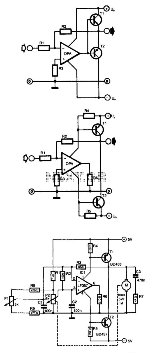
Frequently, the output current of an operational amplifier is inadequate for applications such as driving a small motor or loudspeaker. This issue is typically resolved by adding an emitter follower to the circuit. However, this configuration does not allow...
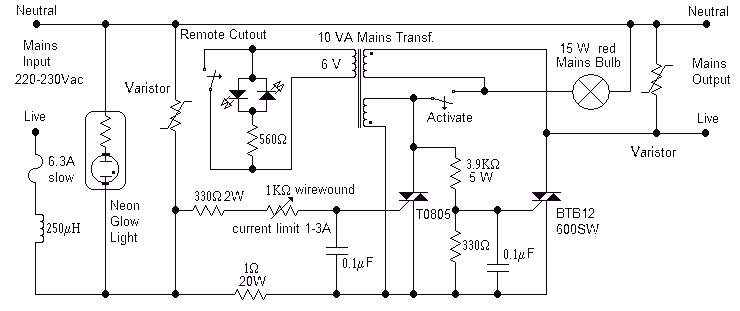
Full short-circuit and overcurrent protection is given by this circuit suitable for workbench applications in technical schools and laboratories where there is a need to work directly with the mains. Additional features are a clearly visible red lamp indicating...