
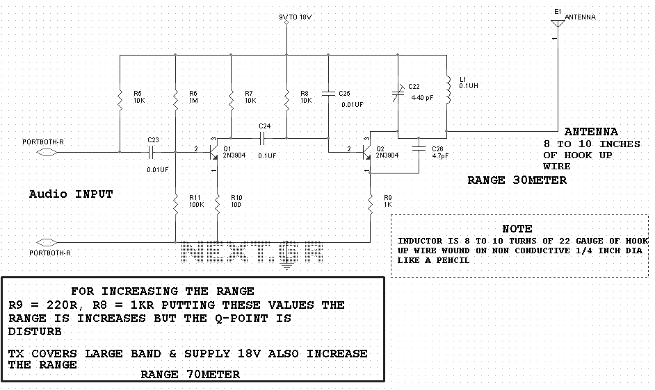
8051 Development System Circuit Board 4
The design of the MP3 player project showcases the complexity involved in memory management when utilizing the 8051 processor. The architecture's limitation of a 16-bit address space necessitates careful planning to ensure efficient use of available memory. The implementation of bank swapping allows for the effective expansion of memory, enabling the system to handle larger datasets, particularly in applications such as data logging and audio streaming.
The use of an AND gate (74AC08) to combine memory spaces simplifies the design, facilitating easier integration and management of memory resources. By employing techniques such as connecting higher address bits to port pins, the design achieves a flexible memory architecture that can adapt to various requirements. The transition from the 39F512 to the 39F040 flash ROM further enhances memory capacity, providing options for extensive data storage through the utilization of multiple banks.
However, the challenges associated with bank-swapped memory highlight the need for careful coding practices, especially in relation to variable allocation and access. The potential for incorrect data retrieval underscores the importance of understanding the nuances of memory management within the context of the 8051 architecture. Overall, the project illustrates the balance between expanding memory capabilities and maintaining system stability, a crucial consideration in embedded system design.There are some important considerations to using more memory, but it certainly is possible. the mp3 player project uses 32 megabytes! But using more memory requires careful consideration. The most important factor is that the 8051 processor has a 16 bit address space. This means the processor can never "see" more than 64k of memory. Actually, the 8051 has three memory spaces, 256 bytes of internal RAM, and two 64k byte external spaces, one for data and the other for executable code. The executable code space is read-only (PSEN signal), so there is really only one writable 64k address space. This design uses an AND gate (74AC08) to combines the two spaces together, which makes the board simpler to use and of course is needed to allow writing to the memory during code download.
So in the end, there is really only a 64k address space to use. A common approach to using more memory is to connect the memory as shown above, and then to connect the higher address bits (A16, A17, etc) to port pins. This is called "bank swapping", because it effectively provides multiple banks of memory and only one is "visible" to the processor at any one time.
The banks are "swapped" by changing the port pins that connect to the upper address bits. In the schematic above, the 39F512 flash rom is actually 64k of memory, but only 30k is available to the user (the chip select logic does not assert CE, pin 22, so that the LCD, 82C55 and chip select signals can use the upper 2k of the memory map). A simple approach to using 60k of flash memory would be to disconnect A15 (pin 3) from +5V and attach it to one of the port pins.
Likewise, a 39F040 chip could be substituted for the 39F512, and then A16, A17, and A18 could be attached to additional port pins to provide sixteen banks of 30k or a total of 480k of flash memory. A similar approach could be used with the RAM chip, as there are 128k and 512k RAM chips. These larger RAM chips have 32 pins instead of 28 pins, but their 28 common pins have similar functions, so only a few extra pins need to be connected.
Again, connecting upper address bits to the port pins would allow the memory to be "bank swapped". Bank swapped memory is most suitable for storing data, such as a data logging application where sensors are read and their data is collected and stored into the flash rom, and later read out when the user collects it to their PC. The MP3 player uses megabytes of RAM to hold MP3 bitstreams that have been read from the hard drive and are waiting to be played by the decoder chip.
Bank swapped memory is not suitable for normal program variables. When the SDCC C compiler allocates a variable in the RAM chip (xdata keyword, which is the default type if you use the large memory model option), the compiler does not "know" about bank swapping. If you change that port pin and the compiler attempts to access any variable in the RAM chip, it will access incorrect information.
It is possible to write an application entirely in assembly that makes only proper accesses to bank swapped variables, but it is difficult to write this sort of code. A similar problem occurs when the flash rom is used for both executable code and data logging. The data logging portion can be bank swapped, but the code portion must not change because any change while code is executing would cause the program to crash.
There are some creative approaches to write code to deal with these issues, but usually the best approach is to avoid bank swapping for program code and especially for normal program variables. Often a more sophisticated approach to bank swapping is needed, where a portion of the address space is always the same, and the rest is bank swapped.
For example, a 74HC08 AND gate chip could be used between those port pins and the upper address bits (A15, A16, A17, A18) of a 39F040 chip. 🔗 External reference
Related Circuits
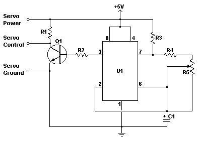
Servo motors are utilized in various applications, including robotics, puppetry, photography, and more. These compact motors can adjust their output shaft to a specified position on command and maintain that position. Most servos offer a range of motion of...
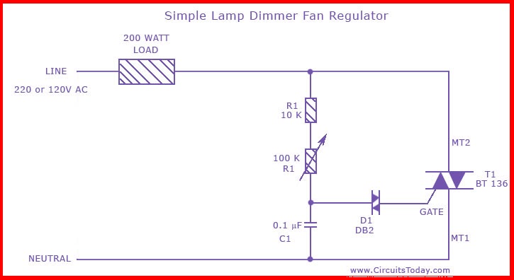
This is the circuit diagram of the simplest lamp dimmer or fan regulator. The circuit is based on the principle of power control using a Triac. The circuit operates by varying the firing angle of the Triac, which is...
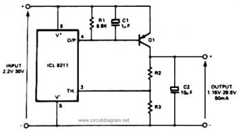
The IC8211 serves as a voltage reference and regulator amplifier, with Q1 likely functioning as the series pass transistor. R1 determines the output current of the IC8211, while C1 and C2 contribute to loop stability and help suppress the...

Figure 1-122 is a dedicated high-fidelity surround sound processing integrated circuit (IC) TDA3810 circuit that manages surround sound. The stereo signal is processed through input coupling capacitors C1 and C2. The internal buffer amplifier handles the left and right...
The power amplifier Hi-Fi OCL 120W RMS is designed to operate effectively when paired with a suitable power supply circuit and 8-ohm speakers. This circuit exclusively utilizes transistors without any integrated circuits, resulting in a clean sound output. The...
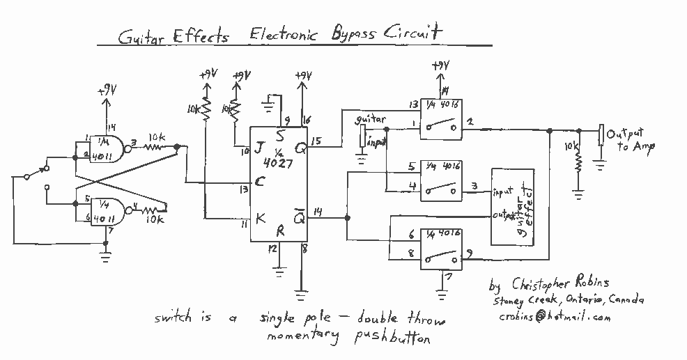
Observing my Boss pedals and how they were switched on and off I figured there must be more to it. It took me only about 4 hours to design and test this circuit. It works very well and I’m...