
902Mhz-cw-transmitter
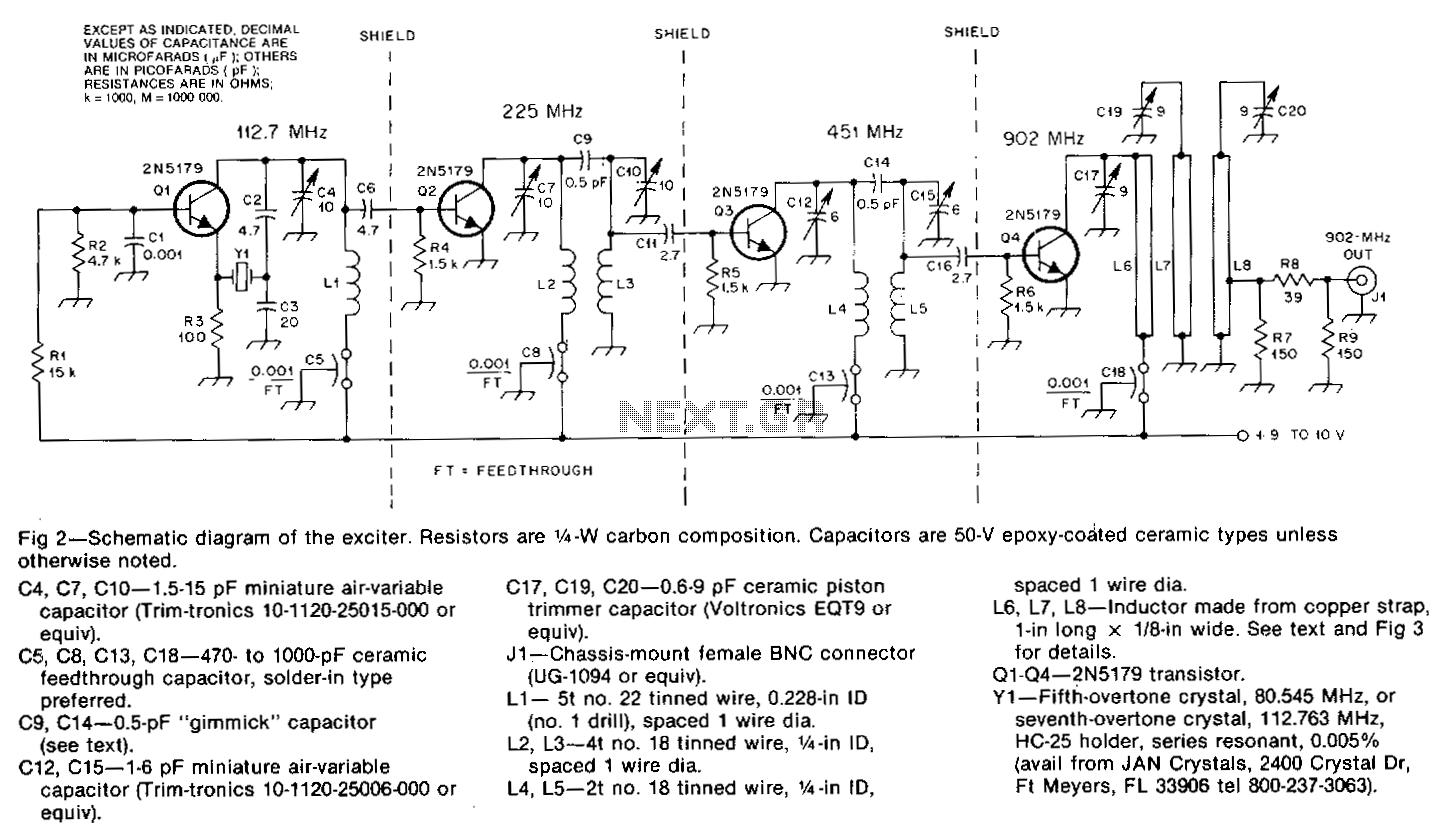
The oscillator, Q1, is a standard overtone circuit. A fifth-overtone crystal, 80.545 MHz, is operated on the seventh overtone, 112.763 MHz. C6 couples the output of the oscillator to Q2, which operates as a doubler to 225.5 MHz. A double-tuned circuit using C7, L2, L3, and C10 is used in the collector of Q2 to reduce the level of the 112-MHz oscillator signal. The output of Q2 is capacitively coupled at C11 to the base of Q3. The double-tuned circuit in the collector of Q3 with C12, L4, L5, and C15 is tuned to 451 MHz. A small capacitance of 2.7 pF couples the 451-MHz signal to the base of another 2N5179, Q4, which doubles the signal to 902 MHz. The output of the 902-MHz doubler has a triple-tuned circuit using C17, L6, C19, L7, C20, and L8 in its collector.
The described circuit comprises a multi-stage frequency doubling arrangement utilizing standard overtone oscillators and tuned circuits to achieve high-frequency outputs. At the initial stage, Q1 serves as the oscillator using a fifth-overtone crystal, operating at 80.545 MHz, and generating a fundamental frequency at the seventh overtone, which results in an output frequency of 112.763 MHz. The output from Q1 is coupled to Q2 through capacitor C6, which serves to block DC while allowing the AC signal to pass. Q2 functions as a frequency doubler, effectively doubling the input frequency to produce a 225.5 MHz output.
In the collector of Q2, a double-tuned circuit composed of capacitors C7, C10 and inductors L2, L3 is implemented. This configuration is crucial for filtering and reducing unwanted harmonics, specifically targeting the suppression of the 112 MHz oscillator signal, thereby improving the purity of the output signal.
The output from Q2 is then capacitively coupled to the base of transistor Q3 via capacitor C11. Q3, configured similarly to Q2, operates with a double-tuned circuit in its collector, consisting of C12, L4, L5, and C15, which is precisely tuned to 451 MHz. This tuning is essential for maximizing the efficiency of the frequency doubling process.
To couple the output of Q3 to the next stage, a small capacitance of 2.7 pF is used to transfer the 451 MHz signal to the base of another transistor, Q4, which is also a 2N5179. Q4 further doubles the frequency, resulting in an output frequency of 902 MHz. The collector of Q4 incorporates a triple-tuned circuit consisting of capacitors C17, C19, and inductors L6, L7, L8, which serves to filter and refine the output signal, ensuring it meets the desired frequency specifications while minimizing spurious emissions.
This multi-stage design effectively illustrates the use of overtone oscillators and tuned circuits to achieve high-frequency outputs in RF applications. The careful selection of components and their configurations plays a critical role in the performance and efficiency of the overall circuit.The oscillator, Q1, is a standard overtone circuit. A fifth-overtone crystal, 80.545 MHz, is operated on the seventh overtone, 112.763 MHz. C6 couples the output of the oscillator to Q2, which operates as a doubler to 225.5 MHz. A double-tuned circuit using C7, L2, L3, C10 is used in the collector of Q2 to reduce the level of the 112-MHz dscillator signal. The output of Q2 is capacitivelJ: coupled at C11 to the base of Q3. The double-tuned circuit in the collector of Q3 with C12, U, L5, C15, is tuned to 451 MHz. A small capacitance, 2. 7 pF, couples the 451-MHz signal to the base of another 2N5179, Q4, which doubles the signal to 902 MHz. The output of the 902-MHz doubler has a triple-tuned circuit using C17, L6, C19, L 7, C20, L8 in its collector.
🔗 External reference