
A simple AM modulator
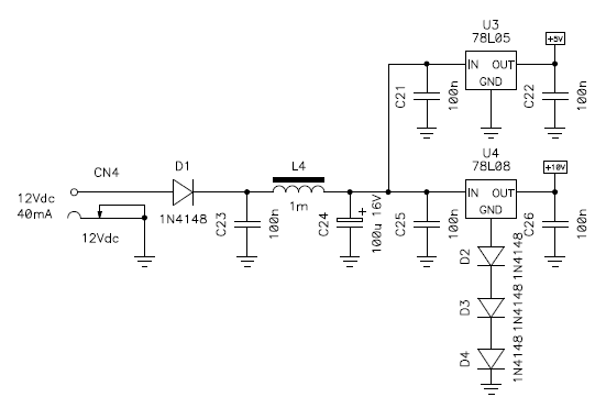
The design of this AM modulator circuit incorporates several key components that ensure stable performance and compatibility with various audio sources. The NE5532 operational amplifier is noted for its low noise characteristics, which is essential for audio fidelity in modulation applications. The input stage's impedance matching is crucial for minimizing signal loss and maximizing audio quality, particularly when interfacing with different output types from audio devices. The use of RC networks to limit the frequency response is a common technique in audio applications, ensuring that only the desired audio frequencies are transmitted while suppressing unwanted low-frequency and high-frequency noise.
In addition, the circuit's reliance on a crystal oscillator for carrier frequency generation enhances frequency stability, which is critical for maintaining clear audio transmission. The choice of a fixed bias voltage for the modulator stage also reflects a thoughtful approach to achieving optimal performance without introducing unnecessary complexity. This design not only serves its primary function of modulating audio signals for AM transmission but also provides a valuable tool for audio testing and troubleshooting in older radio receivers. Overall, this AM modulator circuit exemplifies a well-engineered solution for integrating modern audio playback devices with traditional AM radio technology.An AM modulator for the MW band that will allow hearing the music of a CD or MP3 player during daytime on such radios. This is not a transmitter: the output power is very low (only 10mW) and is intended to be connected to the antenna input of the radio, or to be closely coupled with it.
Amplifying the signal would be a bad idea, since transmitting in this band is strictly forbidden in many countries. The audio signal is connected to CN1 and CN2. The input stage is designed for stereo signals of 0. 7Vrms (2Vpp) and has an impedance of 47k © because this is usually what is needed to connect the line output of a CD player. If one wants to use the earphone output of an MP3 player, shorting JP1 and JP2 will drop the input impedance to 33 © to match this kind of output.
AM only supports mono signals, so both channels are just added together in U1:A. In case of connection of a mono signal source, one can use either CN1 or CN2, but should always short the jumper of the other channel to make sure it doesn`t pick up noise. The RC networks C3-R2 and C6-R6 limit the lower side of the bandwidth to about 50Hz preventing DC from shifting the bias of the modulator.
U1 is an ordinary NE5532 low noise audio operational amplifier. U1:A is just an inverting additioner with a gain of -2 (6dB). The network R7-C7 limits the upper part of the bandwidth to about 4. 8kHz. U1:B is an inverting amplifier whose gain can be adjusted via R8 between -0. 45 (-7dB) and -4. 5 (+13dB). This is used to adjust the modulation factor as close as possible to 100% according to the exact amplitude of the input signal. To avoid distortion, 80% will be good enough, since power efficiency is not an issue for this application.
If this range is not enough, one could change R9 and R8 to increase or decrease the gain. The network R5-C5 limits again the upper edge of the bandwidth of this amplifier to 4. 8kHz. Capacitors C8 and C9 make sure the inverting inputs of the two operational amplifiers are grounded at RF preventing the operating point to shift because of RF leakages from the modulator stage. R1 and R4 bias both operational amplifiers at about 5Vdc, while bypass capacitors C2 and C4 removes RF leakages from the bias line.
Capacitor C1 is used as energy tank to supply the amplifiers during audio peaks. The output of U1:B directly feeds the modulator stage. The bias of this amplifiers directly controls the bias point of the modulator. It was fixed to 5V to allow voltage swings almost from 0 to 10V. Changing the bias voltage will reduce the maximum undistorted RF amplitude. In this circuit, the carrier frequency is generated by a crystal oscillator. Using a VFO was considered for its simplicity, but neutralizing thermal drift will make the circuit more complex to adjust and since old radios do also have significant drift, having a stable frequency would simplify its use and allows using this modulator as test equipment for fixing defective receivers. In Europe, AM broadcast stations use a 9kHz channel raster and all carrier frequencies are an integer multiple of 9kHz.
It would be ni 🔗 External reference
Related Circuits
A TV modulator is really no more than a transmitter. It is a very small transmitter, admittedly, but none the less that is what it is. What does a modulator actually do? In general - and this design is...
The circuit was designed to experiment with using small fluorescent lamps as a broad pattern source of modulated light. The circuit delivers narrow 1 μs pulses to the small lamp at a frequency of 10 kHz. Each pulse generates...
The following circuit illustrates a Simple Moisture Detector Circuit Diagram. This circuit is based on the 4093 IC. Features include the ability to detect a certain level of moisture. The Simple Moisture Detector Circuit utilizes the 4093 integrated circuit, which...
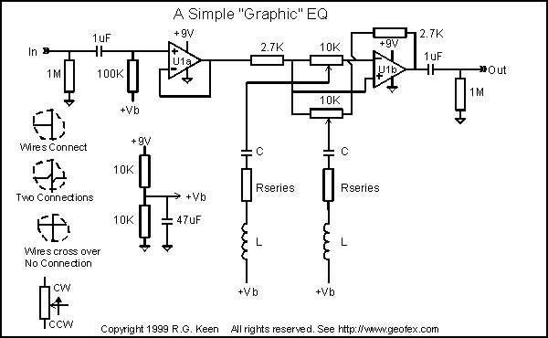
The sound of a wah pedal is characterized by a resonant peak in the signal that can be adjusted. In contrast, a notch represents a sudden decrease in level at a specific frequency, which can be advantageous for achieving...
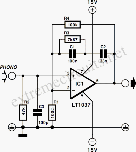
Phonographs are becoming increasingly rare as they are being replaced by more advanced audio systems such as CD players, recorders, and portable MiniDisc player/recorders. This shift is acknowledged by audio equipment manufacturers, leading to the omission of traditional phono...
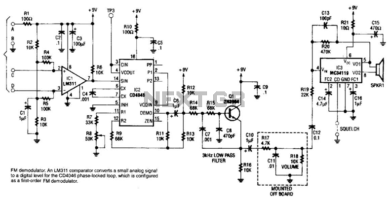
An LM311 comparator converts a small analog signal to a digital level for the DC4046 phase-locked loop, which is configured as a first-order FM demodulator. This demodulator operates with a 50-kHz FM modulated input signal and has applications in...
Warning: include(partials/cookie-banner.php): Failed to open stream: Permission denied in /var/www/html/nextgr/view-circuit.php on line 713
Warning: include(): Failed opening 'partials/cookie-banner.php' for inclusion (include_path='.:/usr/share/php') in /var/www/html/nextgr/view-circuit.php on line 713