
Active Shortwave Antenna PCB
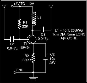
The active shortwave antenna circuit is designed to amplify weak signals within the shortwave frequency range, enhancing the listening experience on compatible receivers. The circuit's architecture is straightforward, relying on a low-noise transistor (T1) that plays a crucial role in signal amplification. The choice of the BF494 or BF495 transistors ensures low noise levels, which is essential for maintaining signal integrity.
Resistor R1, which provides the necessary DC bias, is critical for setting the operational parameters of T1. The specified range of 100 kilo-ohms to 22 kilo-ohms allows for flexibility in tuning the circuit to various environmental conditions and receiver sensitivities. It is essential to maintain R1 within this range to prevent excessive current flow that could lead to thermal overload and potential damage to the transistor.
Resistor R2 is strategically placed to limit the current through T1, ensuring the transistor operates within safe limits. The combination of R2 and capacitor C2 establishes a stable operating point, allowing the circuit to handle variations in signal strength without introducing distortion. The selection of inductor L1 is also significant; as the frequency increases, reducing the number of turns in L1 helps maintain optimal performance and prevents signal loss.
To further enhance the circuit's reliability, a 180 H RFC is included in series with the positive supply rail. This component, along with a bypass capacitor to ground, is crucial for filtering out noise from the power supply, which can adversely affect signal quality. The low current consumption of under 10 mA indicates that the circuit is energy-efficient, making it suitable for portable applications.
The active shortwave antenna circuit is particularly effective in the 13m-49m band, where it delivers satisfactory performance. However, users should be aware that as frequencies approach the upper or lower limits of the shortwave spectrum, the circuit's efficacy diminishes. This characteristic necessitates careful selection of antenna lengths; a long wire for the input antenna and a maximum of 30 cm for the output antenna are recommended to optimize reception quality. Overall, this circuit design offers a robust solution for enhancing shortwave signal reception in a variety of settings.The circuit of active shortwave antenna presented here boosts weak shortwave signals so that these can be heard with enhanced clarity over a shortwave receiver. Further, the receiver doesn`t require any physical connection as its placement in the vicinity (within 6 to 7 cm) of the circuit antenna will suffice.
The circuit works well over a wide ra nge of supply voltage from 3 volts to 12 volts. Low-noise transistor T1 (BF494 or BF495) is connected as shown in the figure. Resistor R1 gives the DC bias to T1. R1`s value may lie anywhere between l00 kilo-ohms and 22 kilo-ohms; it determines the quiescent base-emitter current for transistor T1. Resistor R2 limits the current flowing through transistor T1 and, in conjunction with capacitor C2, determines the operating point for its stable operation.
The number of turns in inductor L1 would have to be reduced as operation area shifts towards the upper end of the high-frequency band. A 180 H RFC in series with positive supply rail, along with a bypass capacitor to the ground, is recommended for reducing signal loss in the power supply.
The current consumption is well below 10 mA. The transistor works well at maximum supply and so reduction of resistor R1`s value below 22 kilo-ohm is not recommended, as otherwise the transistor may burn off. This circuit works satisfactorily for boosting signals in 13m-49m band. However, as the frequency increases, its performance deteriorates. The same happens when the frequency decreases below that of the shortwave range. For input use a long wire as the antenna, while the output antenna wire may be limited to about 30 cm.
🔗 External reference
Related Circuits
This project merges two significant themes from radio history: crystal radios and shortwave (SW) listening. It has been developed from the ground up by non-resident engineer Walter Heskes. Despite advancements in modern electronics, numerous crystal sets are actively used...
City dwellers and other flat dwellers know the practical difficulties they encounter when they try to put up an antenna for 40 meters. Finding space enough to accommodate 67 feet of wire is a real problem for them and...

This antenna tuning unit (ATU) allows half-wavelength or longer wire antennas to be matched to the 50-ohm antenna input of 27-MHz Citizens Band (CB) radios. The ATU is particularly useful in situations where a wire antenna is less visually...

An audio filter is positioned at the input of each audio integrated circuit (IC) chip to filter the audio signal intended for speakers. A low-pass filter is utilized for the woofer, while a high-pass filter is employed for midrange...
The CAD tool for engineering professionals worldwide: CADint PCB gets the job done without getting in your way. Powerful, fast and stable, yet with an ease of use that gets you productive in a hurry. More: All types of...
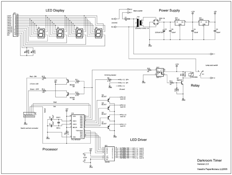
This is an enhanced version of the Darkroom Timer initially developed by Stan Ockers in 1999. Additional features have been incorporated, and the PIC code has been accordingly modified. The complete schematic, PCB layout, and silkscreen are provided in...