
ADC Tester (A2100)
The Probe Auxiliary Board utilizes a THS4130 differential amplifier, providing a single-ended or differential input for the AD7982, allowing for testing of the amplifier's settling time after exiting power-down mode. This configuration enables the A2100 to function as a dual-channel eighteen-bit oscilloscope in future applications. The LWDAQ interface and data memory of the A2100 are derived from the Data Recorder (A3007) developed by Open Source Instruments, but the A2100 is simpler, lacking a RAM FIFO and the capability for simultaneous data storage and retrieval.
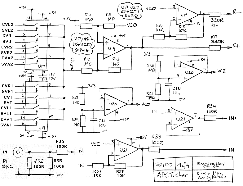
The circuit diagram begins with the RJ-45 connection to the LWDAQ, programmable logic chip, reference oscillator, clock oscillator, and 512-KB static RAM. The auxiliary board for LTC1865L features a fully-differential input in an MSOP-10 package, with switched reference and analog supplies set to 5V for the faster LTC1865. The A2100 adheres to the LWDAQ Specification in all respects except for current consumption, categorized as LWDAQ Device Type 3 (DATA), and it does not implement element numbers.
The command bit allocation includes an LB bit for enabling logic signal return and inhibiting analog return, which is used to monitor current supplied by auxiliary board fixed voltages. The DTX bit enables byte transfer from the device to the driver, which initiates transmission of each byte upon receiving a stop bit. The device transmits the first byte of sample data after the sampling session concludes, with subsequent bytes transmitted following additional stop bits. If not sampling, the device transmits data immediately after receiving a stop bit.
The DRX bit activates the top eight command bits as an instruction, with bits I0 to I7 forming an eight-bit instruction. The A2100 executes instructions upon receiving a command word with DRX set to one. Each ADC contributes four bytes to the data stream: one byte for the ADC number and three bytes for the ADC sample. This design allows for future configurations with more than two ADCs while using the same data acquisition software.
The A2100 operates with a nineteen-bit data address to read from and write to RAM. Data address increments occur with each byte stored or read. At the end of a sampling session, the data address resets to zero. Simultaneous reading and writing of data are not supported; during sampling, the RAM is dedicated to data storage, making it available for download only after the session concludes.
The command word's top eight bits serve as instructions only when the DRX bit is set. Instructions consist of an operation and an argument, both four bits long. The SSS operation initiates a sample session, recording samples based on the number determined by the sample code and the sample rate code set by NSC and SRC operations. The SFV operation controls the fixed voltages supplying power to the auxiliary boards, while the RST operation resets the device's state.
The current measurement channel can select from eight channels, with six measuring currents delivered to the auxiliary boards and two for top and bottom reference currents. An analog multiplexer selects the channel, with amplifiers driving the measurement voltage. The command word required to select each channel must have LB set to 0 to enable the analog return and DRX set to 1 for instruction execution.
The VB and VT channels return the bottom and top reference current measurements, respectively, with resistor values determining the reference current. The A2100 allows for current measurements to be read, analyzed, and displayed using the Gauge Instrument, which can be configured through the LWDAQ software. The dynamic range for current measurement is 50 mA, with optimal performance at currents below 25 mA to prevent overheating of regulators.
To initiate a sample session, the SSS operation is used, with the session continuing until an RST operation is received if the number of samples code is zero. Each sample occupies eight bytes, and the A2100 resets its data address to zero after completing a session, preparing it for the next data upload.
The actual number of recorded samples exceeds those indicated in the documentation, simplifying binary logic and expediting firmware compilation, which is designed for efficiency.The ADC Tester (A2100) is a LWDAQ device that records the output and power consumption of two ADC s. Its original purpose was comparative testing of two ADCs at different temperatures, but it turned out that the A2100 makes a good dual-channel eighteen-bit oscilloscope. Figure: ADC Tester (A2100A) with Two LTC1865L Auxilliary Boards. The flex cabl es are short for the benefit of the photograph. We give the names of the four indicator LEDs. (1) RJ-45 connection to LWDAQ, (2) programmable logic chip, (3) 512KG—8 static RAM, (4) Analog signal input, (5) ADC1 auxilliary board, (6) ADC2 auxilliary board, (7) Pt 1000 RTD glued to LTC1865L, (8) connection for two additional RTDs, (9) 12-way flex cable, (10) fixed voltage supplies for ADC2, (11) fixed voltage supplies for ADC1, (12) logic programming connector, (13) connection to Resistive Sensor Head ( A2053L ). The two ADCs do not reside upon the A2100. They reside on auxilliary boards, which are separate, miniature circuit boards connected to the A2100 by 12-way, 1-mm pitch, 25-cm long flex cables.
In a sampling session, the A2100 takes simultaneous, regular samples from both ADCs and stores them in its 512 KByte memory. Once the sampling session is over, we can read out some or all of the samples and analyze them. We control and read out the A2100 with our LWDAQ Software. We use the program`s Terminal Instrument to define sampling sessions and read out blocks of ADC samples.
We use the Gauge Instrument to measure the currents supplied through the fixed voltages. Note: We designed the A2100 to compare the response of two ADCs at different temperatures when presented with the same input. In particular, we wanted to study the performance of the AD7982 at ’140 °C. The AD7982 is an 18-bit, 1 MSPS, serial-interface, differential-input ADC in an MSOP-10 package. In case the AD7982 failed at low temperatures, our hope was that the A2100 combined with new auxilliary boards would allow us to test other ADCs as well, one of which might work at low temperatures.
We produced three auxilliary heads for these ADC tests: one each for the AD7982, LTC1865, and AD7980. The resistive sensor connections allow us to put one resistive sensor on each auxilliary head. We use 1000- © platinum RTD s to measure the temperature of the auxilliary heads. The ones we used in these experiments were all purchased from Enercorp. The sensor elements are a thin film of platinum deposited on a ceramic base. The element`s steel wires are soldered to teflon-insulated leads. (The teflon-insulated leads were part of a custom order from Enercorp. ) We will need to know the temperature of the auxilliary boards to ±5 °C from ’140 °C to 30 °C. We will not include resistance-measuring electronics on the A2100. Instead, we will connect the RTDs to a Low-Temperature Head ( A2053L ) by means of a separate connector on the A2100.
Figure: ADC Tester (A2100A) with Auxilliary Boards and Low-Temperature Head ( A2053L ). When we took the picture, we had just cooled ADC2 by immersion in liquid nitrogen, and now the ADC is warming up as it sits above the surface of the liquid. (1) Liquid nitrogen, (2) ADC2 above the liquid, (3) flex cable, (4) ADC1 at room temperature, (5) input from function generator, (6) LWDAQ connection for A2100, (7) RTD cable, (8) LWDAQ connection for A2053L, (9) the Low-Temperature Head (A2053L).
The Probe Auxilliary Board uses a THS4130 differential amplifier to provide a single-ended or differential input for an AD7982 eighteen-bit ADC. The board allows us to test the eighteen-bit settling time of the THS4130 after it comes out of its power-down mode.
In the future, the Probe Auxilliary Board allows the A2100 to act as a dual-channel eighteen-bit oscilloscope. The A2100`s LWDAQ interface and data memory are based upon those of the Data Recorder ( A3007 ) designed by Open Source Instruments.
The A2100 is simler than the A3007 in that it does not implement a RAM FIFO, nor does it allow simultaneous storing and retrieval of data. S2100_1 : First page of circuit diagram showing RJ-45 connection to the LWDAQ, programmable logic chip, reference oscillator, clock oscillator, and 512-KB static RAM.
S2100_6 : Auxilliary board for LTC1865L with fully-differential input in MSOP-10 package. Switch reference and analog supplies to 5V for the slightly faster LTC1865. The A2100 conforms to the LWDAQ Specification in every respect except that of current consumption. It is LWDAQ Device Type 3 (DATA). It implements no element numbers. We give its command bit allocation below. The LB bit enables the logic signal return from the device and inhibits the analog return. The analog return is used to monitor the current supplied by the auxilliary board fixed voltages. The DTX bit enables byte transfer from the device to the driver. The driver will provoke transmission of each byte by sending a stop bit. When the device receives the stop bit, it waits until its current sampling session comes to an end, and transmits the first byte of the sample data. Subsequent stop bits from the driver cause the transfer of subsequent bytes. If the device is not currently sampling, it transmits the byte immediately after receiving the stop bit.
The DRX bit causes the top eight command bits to be used as an instruction. Bits I0 to I7 form an eight-bit instruction. The A2100 will executes instructions immediately after it receives a command word with DRX set to one (see below ). As you can see from the table, byte ordering is big-endian. Each ADC accounts for four bytes. One byte is the ADC number. The other three bytes are the ADC sample. We use one byte for the ADC number so that later permutations of this circuit can have more than two ADCs but use the same data acquisition software.
The A2100 reads from and writes to the RAM location pointed to by its nineteen-bit data address. Each time it stores a byte, it increments the data address. Each time it reads out a byte, it increments the data address. At the end of a sample session, the A2100 resets its data address to zero. The A2100 does not support simultaneous reading and writing of data. During a sample session, the RAM is monopolised by data storage. At the end of the sample session, the bytes are available for download by the driver. The top eight bits of a command word act as an instruction if and only if the command word`s DRX (or DC6) bit is set. Instructions contain an operation and an argument. Both are four bits long. The operations and arguments have the following meanings. An SSS operation starts a sample session. The sample session records a number of samples determined by the number of samples code at a rate determined by the sample rate code.
We set these codes with the NSC and SRC operations. The SFV operation switches on or off the fixed voltages that supply power to the auxilliary boards. On power-up, and after a RST operations, the fixed voltages are turned on. The SFV operation allows us to turn off the fixed voltages if required by our current measurement calibration. The RST operation aborts the current sampling session, sets the data address to zero, sets the number of samples code to zero, sets the sample rate code to zero, sets the current measurement channel to zero, and turns on the fixed voltages.
The current measurement channel selects one of eight current measurement channels for analog return, as shown in the following table. We set the current measurement channel with the CMC operation. There are eight channels in all. Six provide measurement of the six currents delivered to the auxilliary boards (see schematic ). Two provide top and bottom reference currents. An analog multiplexer selects the channel and amplifiers drive the analog measurement voltage onto R+ and R ’ (see schematic ).
The table above gives us the sixteen-bit command word we must transmit to select each channel. This command word must have LB (or DC7) set to 0 so as to disable the device`s logic return and permit its analog return to propagate back to the driver. The command word must have DRX (or DC6) set to 1 so that the A2100 will execute the instruction contained in I7.
I0 (or DC16. DC9). The VB channel returns the bottom reference current measurement, which will correspond to 0 mA or some other lower reference current chosen during assembly. Resistor R31 sets the bottom reference current. The VT channel is the top reference current, set by R29. The VR1, VA1, and VL1 channels monitor the current drawn by the voltages supplied to the first auxilliary board.
The VR2, VA2, and VL2 channels do the same for the second auxilliary board. We read out, analyze, and display the current measurement channels using the Gauge Instrument. We configure the Gauge Instrument to work with the A2100 by changing its gauge_commands string. We set this to the list of commands given in the table above. At the TCL console in our LWDAQ program, you could enter the following line. We also set the Gauge`s ref_top_y and ref_bottom_y parameters to match the top and bottom reference currents that flow through R29 and R31 respectively (see schematic ). Because R29 and R31 are marked TBD (to be decided) on the schematic, you will have to look at your A2100 and determine their values.
In both cases, the reference current is 15/R, where R is the actual value of the resistor. In this calculation, we ignore the value of the current-sensing series resistor, which is 47 ©. With R29 = 10k ©, set ref_top_y to 1. 500 to indicate 1. 500 mA. With R31 = 0 ©, set ref_bottom_y to 0 to indicate 0 mA. The dynamic range of the current measurement is 50 mA. The regulators will start to over-heat if you draw more than 25 mA. We obtain our best results with the Gauge Instrument`s display_s_per_div (shown as Scale s/div in window) set to 0. 001. Current resolution is 1 A. Accuracy over 0 mA to 25 mA is better than 0. 5%. We start a sample session with the SSS operation. If the number of samples code is zero, the sample session will continue until the A2100 receives an RST operation.
Otherwise, the sample session will terminate when the required number of samples has been recorded in memory. As the A2100 records samples, it increments its data address. Each sample takes eight bytes, as shown above. At the end of a sample session, the A2100 resets its data address to zero, and is ready to upload its memory contents to the driver.
Note: The actual number of samples recorded by the A2100 is slightly higher than the number given in the table above. Instead of 50 samples, the A2100 records 64. Instead of 50000, it records 50176. The actual numbers simplify our binary logic. Our firmware is full of such simplifications because we like it to compile fast. The P2100A04. able code compiles in a five seconds. 🔗 External reference
Related Circuits
The MAX1496 is an analog-to-digital converter (ADC) that incorporates LED drivers, allowing for the construction of a 3 1/2 digit voltmeter using a minimal number of components. This device features both external and internal voltage reference options, along with...
You do not need access to advanced testing equipment to check and troubleshoot computer data cables. Instead, this simple device will provide a quick indication of the status. This device functions as a basic cable tester, designed to assess the...
This is a variation on the astable multivibrator. Circuit was recently developed to test for N-mosfets (the power kind e.g. irf830). I don't claim circuit can test all bad mosfets or all fault mosfet conditions. If mosfet is working...
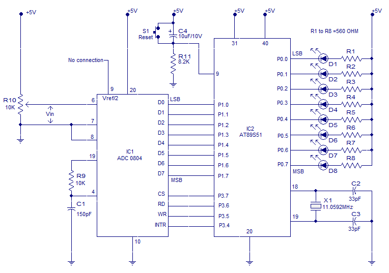
Interfacing ADC to 8051 microcontroller. ADC0804 is interfaced to microcontroller AT89S51. Complete circuit, theory and program in assembly language. The interfacing of an Analog-to-Digital Converter (ADC) with a microcontroller is a critical aspect of embedded systems design, particularly when analog...
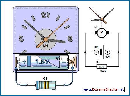
The circuit described is suitable for indicating the capacity of a battery using a low-cost electric clock. By connecting a resistor across the battery terminals, the battery discharges at a faster rate than it would with the clock alone....

Author Jim Walker describes a very low-cost analog delay line circuit using components such as the LM311 comparator and 74HC74 D flip-flop. The analog delay line circuit presented by Jim Walker utilizes the LM311 comparator and the 74HC74 D flip-flop...
Warning: include(partials/cookie-banner.php): Failed to open stream: Permission denied in /var/www/html/nextgr/view-circuit.php on line 713
Warning: include(): Failed opening 'partials/cookie-banner.php' for inclusion (include_path='.:/usr/share/php') in /var/www/html/nextgr/view-circuit.php on line 713