
Add-on-scope-multiplexer
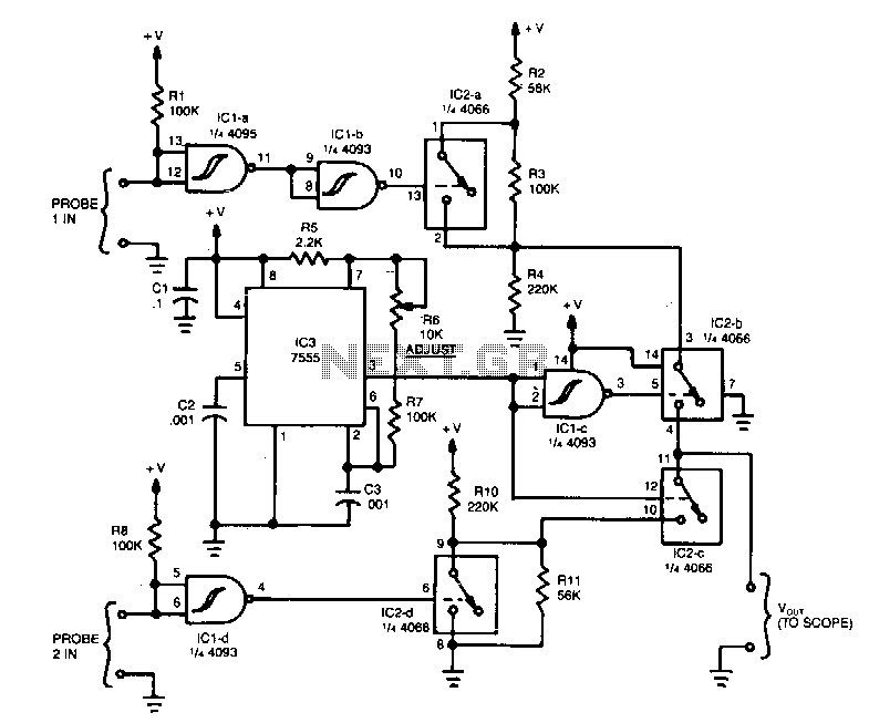
The operation of the unit revolves around three integrated circuits (ICs): a 4093 quad NAND Schmitt trigger, a 4066 quad analog switch, and a 7555 timer. When a high signal is applied to probe 1 input, it is inverted by IC1a and again by IC1b, resulting in a high input to IC2a. This high input causes the switch contacts in IC2a to close. With the contacts closed, a high-level output is presented to the input of IC2b. The high output is then fed to probe 2 input. This signal is then inverted by IC1d and routed to IC2d, causing its contacts to open, which results in the unit outputting a logic-level high. The output of IC2d is then fed to IC2c.
The described circuit utilizes three specific integrated circuits to perform its intended functions effectively. The 4093 quad NAND Schmitt trigger serves as a key element in shaping the input signals. It provides hysteresis, which is beneficial for eliminating noise and ensuring stable switching behavior. The configuration involves two stages of inversion through IC1a and IC1b, which reinforces the signal integrity before it is processed by the next stage.
The 4066 quad analog switch is used to control the flow of the signal based on the logic levels determined by the previous stages. When the input at probe 1 is high, the corresponding output of IC2a is also high, which leads to the closing of the switch contacts. This action allows the signal to pass through to IC2b, effectively enabling the next stage of the circuit.
The 7555 timer, which is a versatile timer IC, can be configured in various modes such as monostable or astable. In this configuration, it appears to be utilized in conjunction with the other ICs to manage timing and control the output states. The output from IC2b is then directed to probe 2, which further processes the signal.
The inversion of the signal by IC1d serves to prepare the output for the next stage, IC2d. When the contacts of IC2d are opened, it indicates a transition to a logic-level high output. This output is crucial for the final processing stage, where it is fed into IC2c, potentially for further logic operations or as a final output signal.
Overall, this circuit exemplifies a sequential logic operation that relies on the interplay between multiple ICs to achieve desired signal processing outcomes. The design effectively utilizes the characteristics of each IC to ensure reliable operation and signal integrity throughout the various stages of processing.The operation of the unit revolves around three !Cs: a 4093 quad NAND Schmitt trigger, a 4066 quad analog switch, and a 7555 timer. When a high is fed to probe 1 in, it is inverted to IC1a and once again by IC1b, so that the input to IC2a is high.
Thathigh causes the switch contacts in IC2a to close. With the contads closed, a high-level output is presented to the input of IC2b. The high output is fed to probe 2 in, That signal is tben inverted by IC1d and routed to IC2d, causing its contacts to open, and tbe unit to output a logic-level high. The output of IC2d is tben fed to IC2c. 🔗 External reference