
Amplifier-for-signal-supply
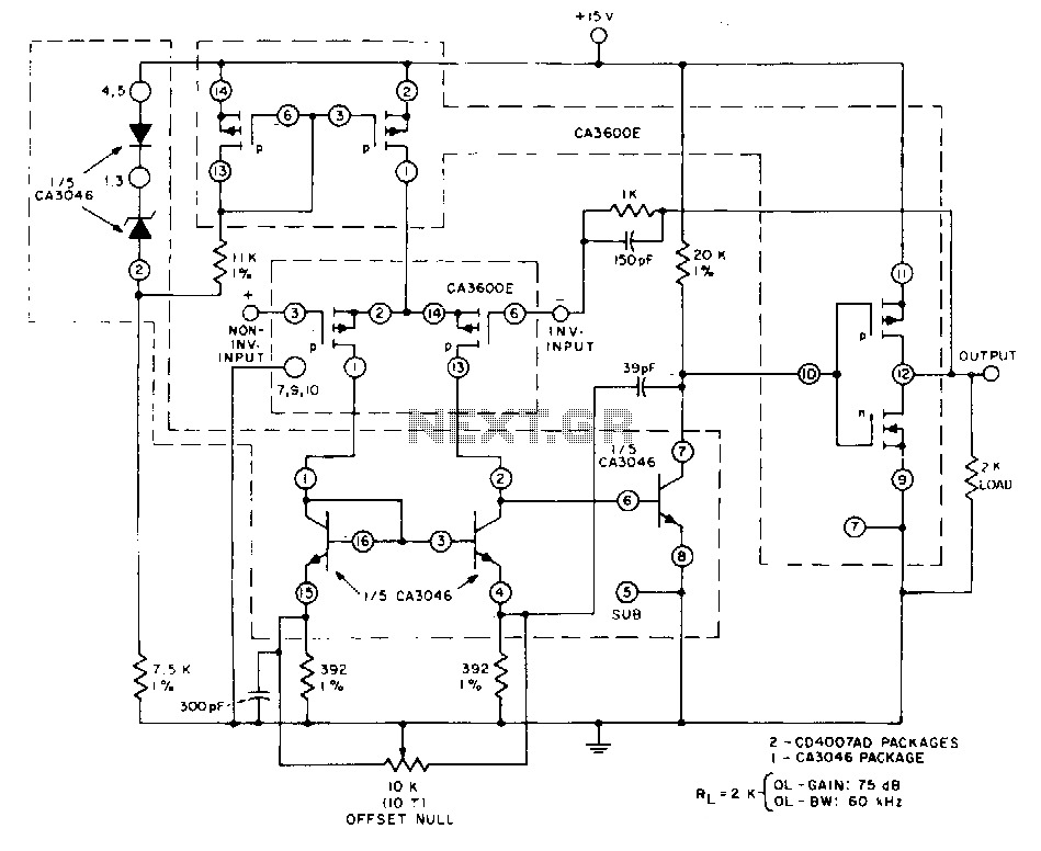
This unity-gain follower amplifier features a CMOS p-channel input, an NPN second-gain stage, and a CMOS inverter output. The integrated circuit components consist of two CA3600E CMOS transistor pairs and a CA3046 NPN transistor array. A zener-regulated leg provides bias for a 400 µA p-channel source, which feeds the input stage that is terminated in an NPN current mirror. The amplifier's voltage offset is adjusted using a 10 kΩ balance potentiometer. The current level of the second stage is determined by a 20 kΩ load, selected to match the first-stage current level to ensure similar positive and negative slew rates. The CMOS inverter section constitutes the final output stage and is terminated in a 2 kΩ load, a standard value for monolithic operational amplifiers. The voltage gain is influenced by the selection of load resistance values. The output stage of this amplifier can be driven to within 1 mV of the negative supply voltage.
The unity-gain follower amplifier design leverages the advantages of CMOS technology, particularly in low-power applications. The CMOS p-channel input stage provides high input impedance and low offset voltage, which is crucial for precision applications. The integration of the CA3600E CMOS pairs allows for efficient signal processing with minimal distortion, while the CA3046 NPN array enhances the overall gain performance through its robust amplification capabilities.
The zener-regulated biasing circuit ensures stable operation of the p-channel source, maintaining consistent performance across varying supply voltages. The use of an NPN current mirror in the input stage aids in maintaining a constant current, which is essential for linear amplification and minimizing distortion.
The balance potentiometer, rated at 10 kΩ, enables fine-tuning of the voltage offset, allowing the user to achieve optimal performance in precision applications. The second stage's current level, set by the 20 kΩ load, is crucial as it matches the first stage's current, thereby ensuring that both stages respond similarly to input signals, which is vital for maintaining linearity and slew rate characteristics.
The final output stage, implemented with a CMOS inverter, is designed to drive a standard 2 kΩ load. This configuration facilitates compatibility with typical monolithic operational amplifiers, ensuring that the amplifier can interface seamlessly with other circuit components. The ability to drive the output stage to within 1 mV of the negative supply voltage is particularly advantageous in applications requiring a wide dynamic range and low distortion.
Overall, this unity-gain follower amplifier design exemplifies a well-engineered solution for applications demanding high precision, stability, and efficiency.This unity-gain follower amplifier has a CMOS p-channel input, an npn second-gain stage, and a CMOS inverter output. The IC building blocks are two CA3600E"s (CMOS transistor pairs) and a CA3046 npn transistor array. A zener-regulated leg provides bias for a 400-I"A p-channel source, feeding the input stage, which is terminated in an npn current mirror.
The amplifier voltage-offset is nulled with the 10-K!l balance potentiometer. The second-stage current level is established by the 20-K!lload, and is selected to approximately theiirst-stage current level, to assure similar positive and negative slew rates. The CMOS inverter portion forms the final output stage and is terminated in a 2-K!l load, a typical value used with monolithic op amps. Voltage gain is affected by the choice of load resistance value. The output stage of this amplifier is easily driven to within 1 mV of the negative supply voltage. 🔗 External reference
Warning: include(partials/cookie-banner.php): Failed to open stream: Permission denied in /var/www/html/nextgr/view-circuit.php on line 713
Warning: include(): Failed opening 'partials/cookie-banner.php' for inclusion (include_path='.:/usr/share/php') in /var/www/html/nextgr/view-circuit.php on line 713