
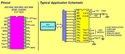
analog to digital converter adc0804
Normal operation commences with a high-to-low transition of the WR input, which resets the internal SAR latches and shift-register stages, setting the INTR output high. As long as the CS and WR inputs remain low, the A/D converter stays in a reset state. Conversion begins one to eight clock periods after either input transitions from low to high. Following the required clock pulses to complete the conversion, the INTR pin transitions from high to low, indicating the availability of a new conversion. A read operation (with CS low) will reset the INTR line high again. The device can operate in free-running mode by connecting INTR to the WR input with CS set to 0. To ensure proper start-up under all conditions, an external WR pulse is necessary during the first power-up cycle. A conversion in progress can be interrupted by issuing a second start command. If the A/D is restarted (CS and WR go low and return high) during conversion, the converter resets and initiates a new conversion. The output data latch will not update if the conversion in progress is incomplete; the previous conversion data remains in this latch. In this configuration, the CS input is grounded, and the WR input is connected to the INTR output. This WR and INTR node should be temporarily set to logic low following a power-up cycle to ensure circuit functionality.
The circuit can be applied in various applications, including magnetic pickup tachometers, serial communication via RS232 using the 8051 program, controlling gate pulses of TRIACs with the microcontroller 8051, and connecting pressure and temperature sensors to an LM324 and microcontroller. Other applications include data acquisition systems using microcontrollers, operational amplifier schematics for data acquisition, control systems utilizing microcontrollers and microprocessors, and graphical display circuits for data acquisition systems. The system can also encompass various electronics projects focused on data acquisition, measurement with microcontroller simulation in Proteus, and interfacing of ADCs such as the ADC0808 and ADC0809 with microcontrollers. Additionally, the circuit can be utilized in digital voltmeter applications using the ADC0804, 8051, and 7-segment LED displays.It is 8-Bit, Microprocessor-Compatible, A/D Converters. Data Collection Analog to Digital Conversion and Communicating and It uses an ADC0804 chip to convert from analog to digital, an AT89C2051. The ADC0802 families are CMOS 8-Bit, successive-approximation A/D converters which use a modified potentiometricladder and are designed to operate with the 8080A control bus via three-state outputs.
These converters appear to the processor as memory locations or I/O ports, and hence no interfacing logic is required. The differential analog voltage input has good common mode-rejection and permits offsetting the analog zero-input voltage value.
In addition, the voltage reference input can be adjusted to allow encoding any smaller analog voltage span to the full 8 bits of resolution. The functional diagram of the ADC0802 series of A/D converters operates on the successive approximation principle.
Analog switches are closed sequentially by successive-approximation logic until the analog differential input voltage [VlN(+) - VlN(-)] matches a voltage derived from a tapped resistor string across the reference voltage. The most significant bit is tested first and after 8 comparisons (64 clock cycles), an 8-bit binary code (1111 1111 = full scale) is transferred to an output latch.
The normal operation proceeds as follows. On the high-to-low transition of the WR input, the internal SAR latches and the shift-register stages are reset, and the INTR output will be set high. As long as the CS input and WR input remain low, the A/D will remain in a reset state. Conversion will start from 1 to8 clock periods after at least one of these inputs makes a low to-high transition.
After the requisite number of clock pulses to complete the conversion, the INTR pin will make a high-to-low transition. This can be used to interrupt a processor, or otherwise signal the availability of a new conversion. A RD operation (with CS low) will clear the INTR line high again. The device may be operated in the free-running mode by connecting INTR to the WR input with CS = 0. To ensure start-up under all possible conditions, an external WR pulse is required during the first power-up cycle.
A conversion-in-process can be interrupted by issuing a second start command. If the A/D is restarted (CS and WR go low and return high) during a conversion, the converter is reset and a new conversion is started. The output data latch is not updated if the conversion in progress is not completed. The data from the previous conversion remain in this latch. In this application, the CS input is grounded and the WR input is tied to the INTR output. This WR and INTR node should be momentarily forced to logic low following a power up cycle to insure circuit operation.
curcuit diagram for magnetic pickup tachometer, serial communication via rs232 using 8051 program, controlling gate pulse of triac by using microcontroller 8051, pressure sensor and temp sensor connected to lm324 and microtroller, daq microcontroller circuits, data acquisition system using mocrocontroller, data acquisition op amp schematic, control system using microcontroller and microprocessor, data acquisition system using graphical display circuit diagram, data acquisition system circuit for ct scan, microcontroller fuzzy logic, electronics projects on data acquisition system, measurement with microcontroller proteus, microcontroller data acquisition systems, what is meant by counter and timer circuit diagram and assembly language program for interfacing of ADC Samples of 89c2051 interfacing with MAX 233/ ADC0804 explain about counter and timer in 8051, "c51" adc0808, circuit diagram for data acquisition, at89s52 proteus, ADC0808 and ADC0809 adc / dac interfaceing, ADC0808 and ADC0809 adc / dac interfacing with microcontroller, Digital Voltmeter Using ADC0804, 8051, and 7 LED Display : 8051 ADC0808 and ADC0809 adc / dac interfacing with 8051, ADC0808 and ADC080 🔗 External reference
Related Circuits
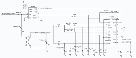
The UC3825 IC, manufactured by Texas Instruments, is a high-speed pulse width modulation (PWM) controller that serves as the central processor for a DC/DC converter control circuit. This circuit primarily consists of three integrated circuits: the UC3825BN, ISO124, and...
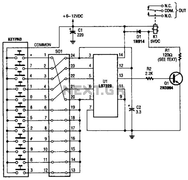
A block pinout diagram of the LS7220 keyless-lock IC is presented. The keypad must provide each key with a contact to a common connection. In this instance, the common connection is linked to the positive supply rail, allowing a...
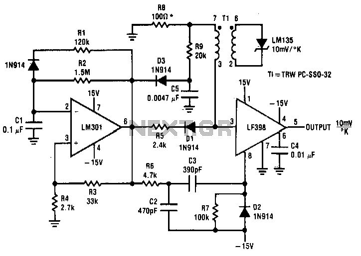
Both converters utilize CMOS inverters. Figure 105-1A illustrates a free-running circuit where both pulse duration and pulse pause are influenced by the temperature of diode D8. This configuration is suitable for applications where synchronization between the converter and other...
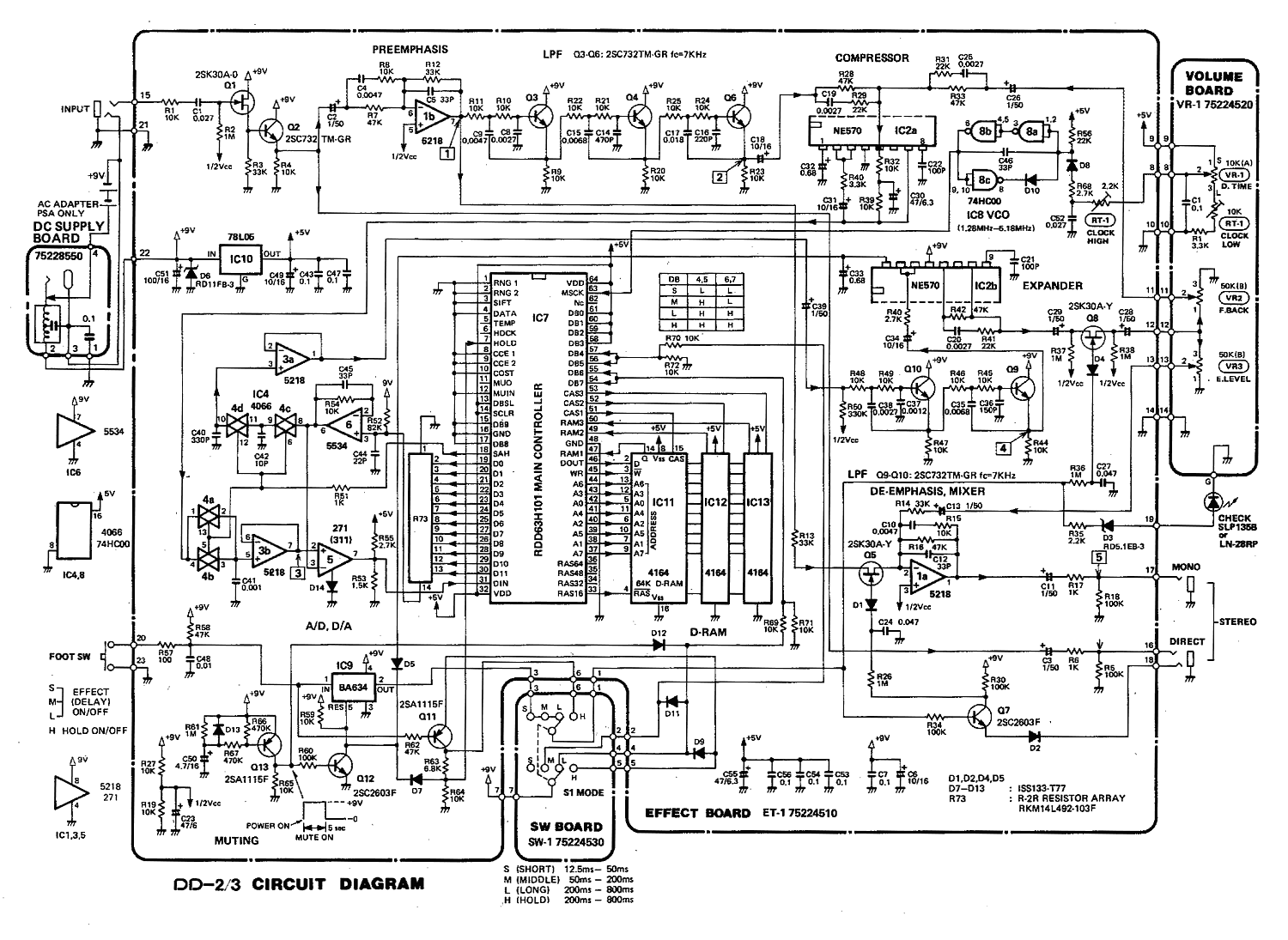
The DD-2 is a highly regarded digital delay pedal that emulates an analog sound. It was initially sold from 1983 until it was discontinued in 1986, after which it was relaunched without any modifications as the DD-3 (noting that...
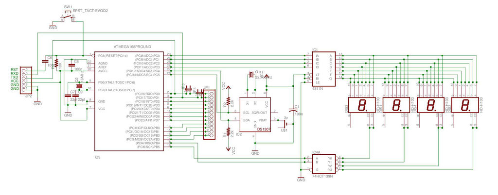
This is the second instructable focused on creating a digital watch as a learning experience. An Atmega644 chip from a Sanguino was available, which would have sufficed, but the intention was to burn an Arduino bootloader and test its...
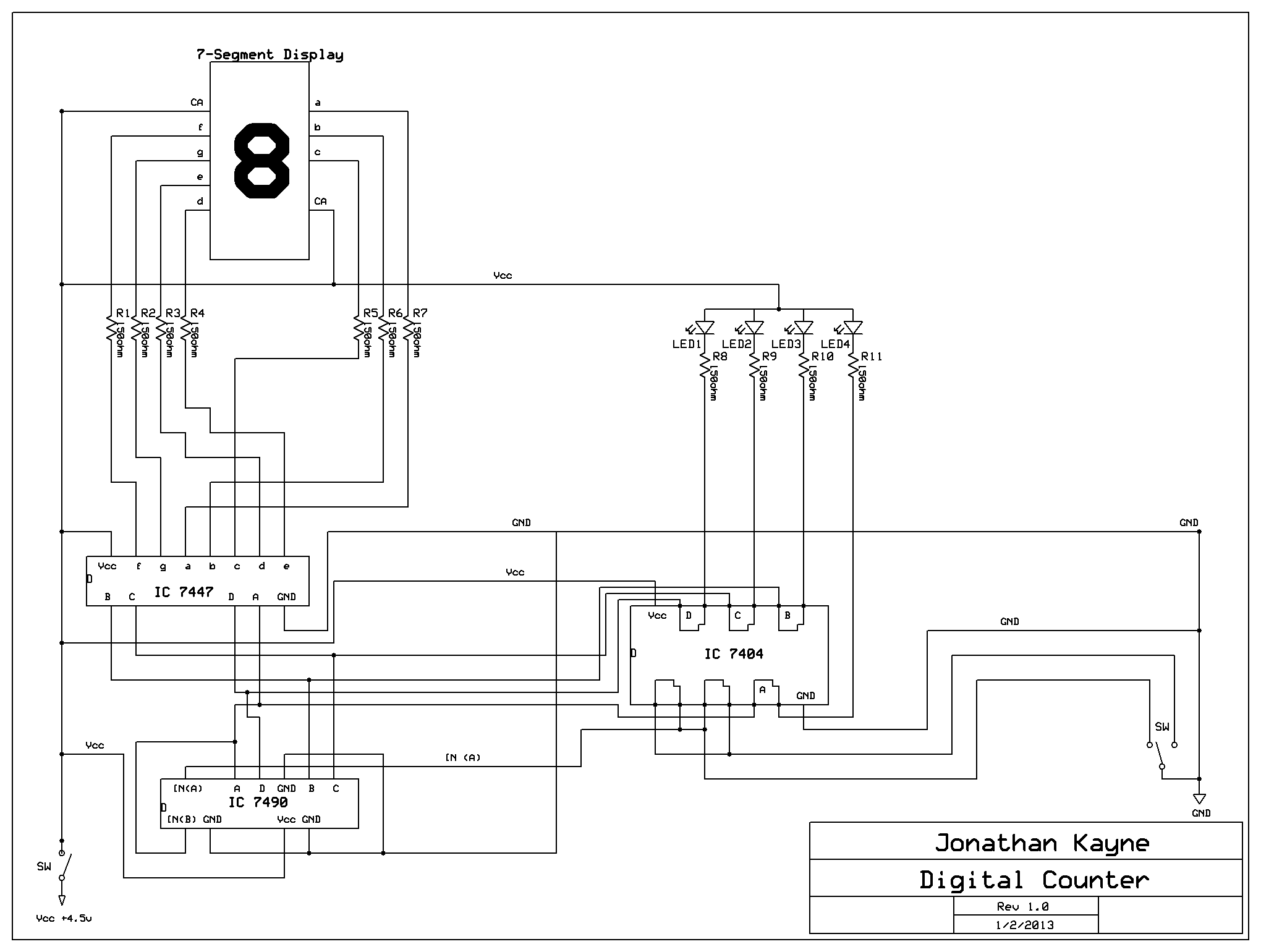
The Digital Counter Circuit is an electronic project that converts digital numbers (0-9) to binary (0-1). For those interested in understanding binary code, a PowerPoint presentation on the topic is available. Below are the parts list, schematic, and additional...