
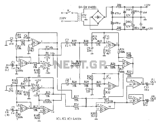
Attenuating a feedback tone control circuit
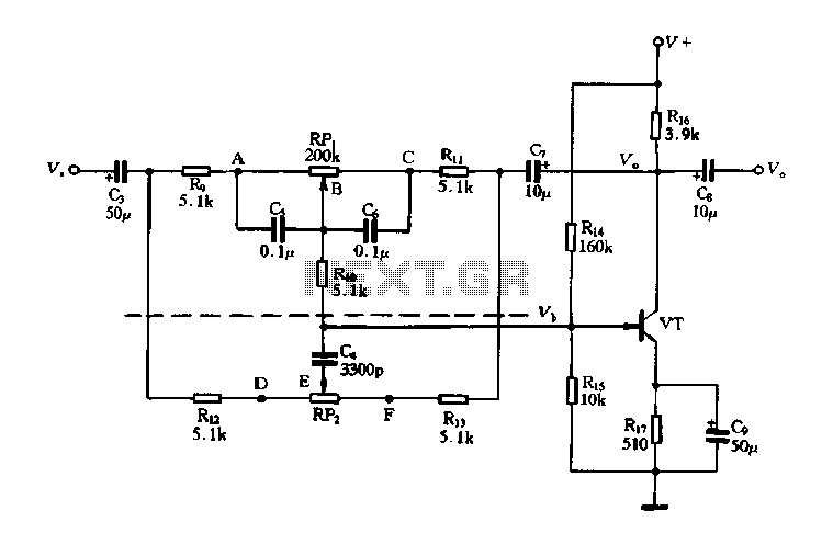
The decay feedback tone control circuit operates by adjusting the frequency response of an audio signal, allowing users to tailor the bass output to their preferences. The anti-attenuation feedback mechanism serves to stabilize the circuit's response, ensuring that the adjustments made to the bass frequencies do not lead to undesirable attenuation of the overall audio signal.
The superposition theorem is applied in the analysis of this circuit to simplify the understanding of its behavior. By considering the contributions of each voltage source independently, it becomes easier to analyze how changes in the input signal (Vi) and the feedback signal (Vo) affect the output. In practical terms, this means that the circuit can be modeled as having separate pathways for the input and feedback signals, enabling a clearer understanding of how they interact.
In the schematic, the input voltage (Vi) is fed into the circuit, where it is processed through various components designed to manipulate the audio signal. The output voltage (Vo) is then fed back into the circuit, creating a loop that allows for continuous adjustment of the bass response. The interaction between these signals is crucial for achieving the desired tonal characteristics, and careful design considerations must be taken into account to ensure that the feedback does not introduce instability or distortion into the audio output.
Overall, the decay feedback tone control circuit exemplifies a sophisticated approach to audio signal processing, leveraging fundamental electrical engineering principles to create an adjustable and responsive tone control mechanism.FIG is a decay feedback tone control circuit. In the tone control circuit both have anti-attenuation Fed action. So high, in the end it is to enhance or attenuate the bass, and sometimes not easy to distinguish. The following theorem using superposition circuit into line analysis. Superposition theorem states that in any linear circuit, the voltage of each branch, can be seen as separately for each source when used in this branch of the voltage generated by the algebraic sum. Figure 1-79 combined analysis, the base of the input signal voltage Vb, can be seen as such by the two sources are the result of the role that the input voltage signal voltage Vi people on the base is formed by an output signal voltage vo negative feedback voltage to the base of the formation.
Related Circuits
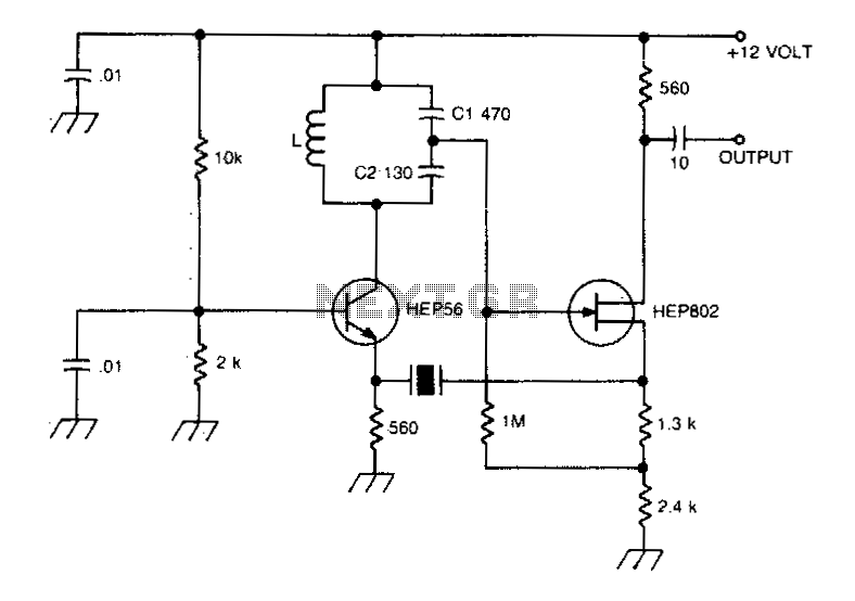
A typical Butler oscillator operating within the frequency range of 20 to 100 MHz incorporates a Field Effect Transistor (FET) in the second stage of its configuration. The circuit exhibits reliability issues when utilizing two bipolar transistors. In some...
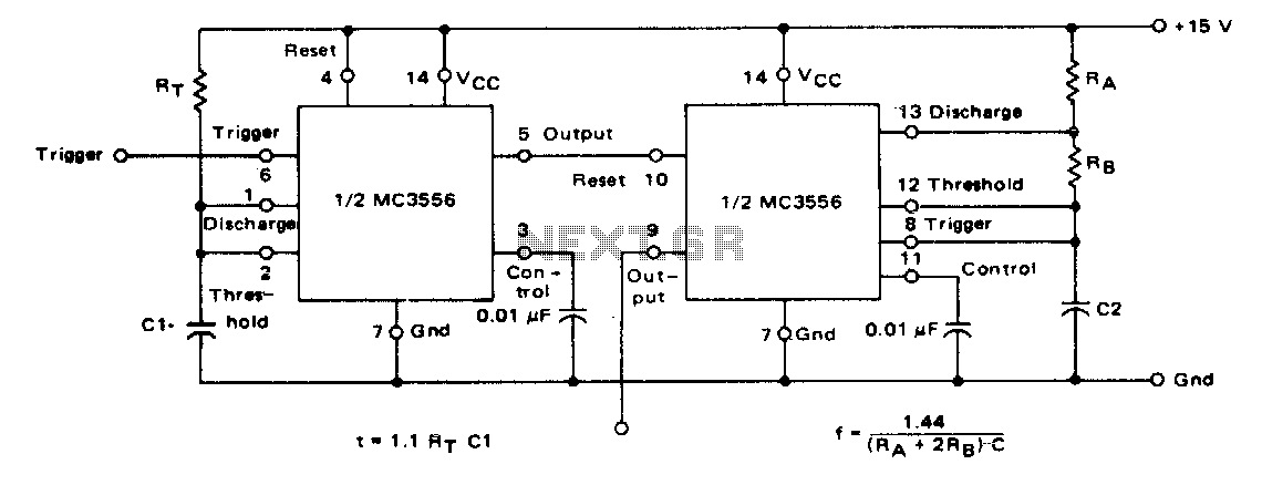
The first timer is used as a monostable and determines the tone duration when triggered by a positive pulse at pin 6. The second timer is enabled by the high output of the monostable. It is connected as an...
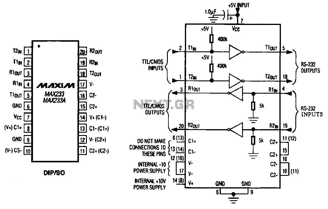
The MAX233 / 233A is a multi-channel data interface circuit featuring dual output and dual input driver circuits. It is designed for small digital products and multimedia equipment to facilitate data transmission. The MAX233 / 233A integrates multiple functions to...
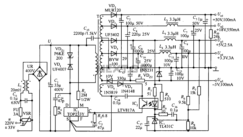
A 35W switching power supply circuit designed for a set-top box output is depicted in Figure 5. It features five distinct voltage outputs: Uo1 (+30V, 100mA), Uo2 (+18V, 550mA), Uo3 (+5V, 2.5A), Uo4 (+3.3V, 3A), and Uo5 (-5V, 100mA)....
The tape output circuit processes the left and right channel signals through a first buffer amplifier. The output signal is split into two paths: one route directly connects to an amplifier for amplification, while the other route passes through...
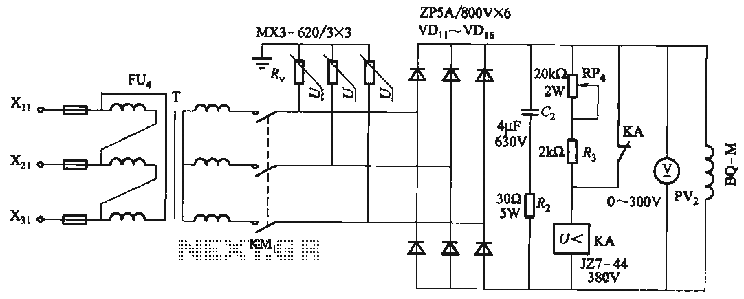
FIG T is the excitation transformer, R is a varistor, and there are rectifier diodes to protect against breakdowns from VDii to VD16; Rz and C2 provide resistive-capacitive protection. The circuit is designed to absorb voltage from the magnetic...