
Audio compressor circuit
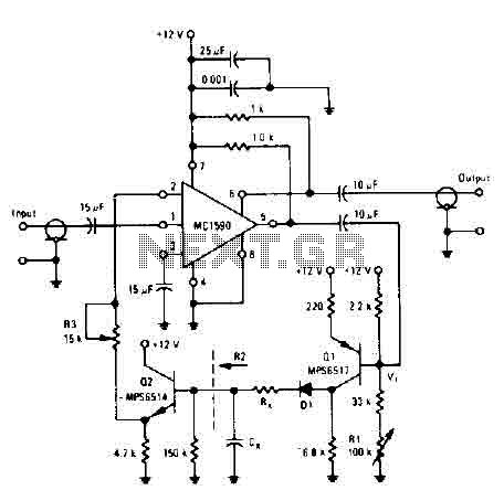
Long and short attack durations are managed by adjusting the values of Rx and R2. An emitter-follower Darlington configuration may be necessary if extremely slow decay times are required. The emitter-follower Q2 drives the AGC Pin 2 of the MC1590, effectively reducing the gain. Resistor R3 controls the slope of the signal compression.
The circuit configuration described utilizes a common emitter PNP transistor (MPS6517) as the primary amplification stage. This transistor is characterized by its ability to provide significant voltage gain, which in this case is set to approximately 20. The RL control mechanism is crucial for setting the quiescent point (biasing) of transistor Q, enabling the circuit to respond dynamically to varying input signal levels. The adjustment of the quiescent point ensures that the transistor operates efficiently within its linear region, allowing for optimal signal amplification.
Diode D1 plays a vital role in signal processing by rectifying the output from Q1, allowing only those positive signal peaks that surpass the threshold of approximately 7.0 volts to pass through. This rectification is essential for further processing the amplified signal, as it converts the AC signal into a pulsating DC signal that can be filtered.
The filtering stage, managed by resistor Rx, is responsible for determining the charging time constant, which directly influences the attack time of the circuit. Capacitor Cx is integral to this process, as it participates in both the charging and discharging cycles, affecting the overall response time of the amplifier.
Resistor R2, with a value of 150 K, acts as the input resistance for the emitter-follower Q2. This configuration is designed to provide a low output impedance while maintaining a high input impedance, which is beneficial for driving subsequent stages in the circuit. The decay time of the output signal is primarily controlled by R2, allowing for fine-tuning of how quickly the circuit responds to changes in input signal levels.
The circuit's design also accommodates the need for adjustable attack times, with the potential for long and short attack durations achieved through the careful selection of resistor values for Rx and R2. In scenarios where extremely slow decay times are desired, the implementation of an emitter-follower Darlington configuration may be warranted, as it provides enhanced current gain and improved performance in such applications.
The output stage, driven by emitter-follower Q2, interfaces with the AGC (Automatic Gain Control) Pin 2 of the MC1590, effectively managing the gain of the overall circuit. Resistor R3 is instrumental in controlling the slope of signal compression, allowing for further refinement of the output signal characteristics in response to varying input levels. This comprehensive design enables the circuit to adapt dynamically to different signal conditions, ensuring consistent performance across a range of applications.The amplifier drives the base of a common emitter PNP MPS6517 operating with a voltage gain of about 20. RL control varies the quiescent point of the transistor Q, so that varying amounts of signal exceed the level of V r, diode D 1 rectifies the positive peaks Ql output is only when these peaks are more larger than r V "'" 7.
0 volts. The result is filtered ex Rx. s, controls the charging time constant or time of attack. Cx is involved in two loading and unloading. R2 (150 K, the input resistance of the emitter-follower Q2) controls the decay time. Making the disintegration of long and short of attack is accomplished by small and large Rx R2. (An emitter follower Darlington may be necessary if the extremely slow decay times are required.) The emitter-follower Q2 drives the AGC Pin 2 of the MC1590 and reduces the gain. R3 controls the slope of signal compression. 🔗 External reference
Related Circuits
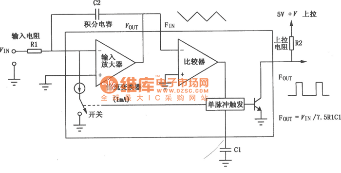
The VFC62 is a voltage-to-frequency and frequency-to-voltage converter that effectively transforms analog signals into digital signals. The digital output is presented in an open collector format, where the digital pulse repetition rate is directly proportional to the amplitude of...
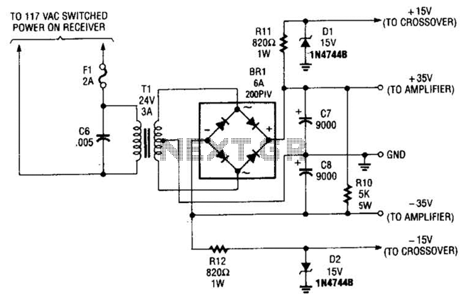
This power supply is designed to power a 100-W low-frequency amplifier and is capable of supporting various mono or stereo amplifiers within the medium power range, specifically those that require 30 to 35 V. The power supply circuit is engineered...
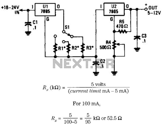
This voltage regulator and current limiter combination can be constructed using two 7805 regulators as illustrated. Resistors R1, R2, and R3 should be chosen to achieve a 5-V drop at the maximum allowable current limit. Switch S1 selects one...
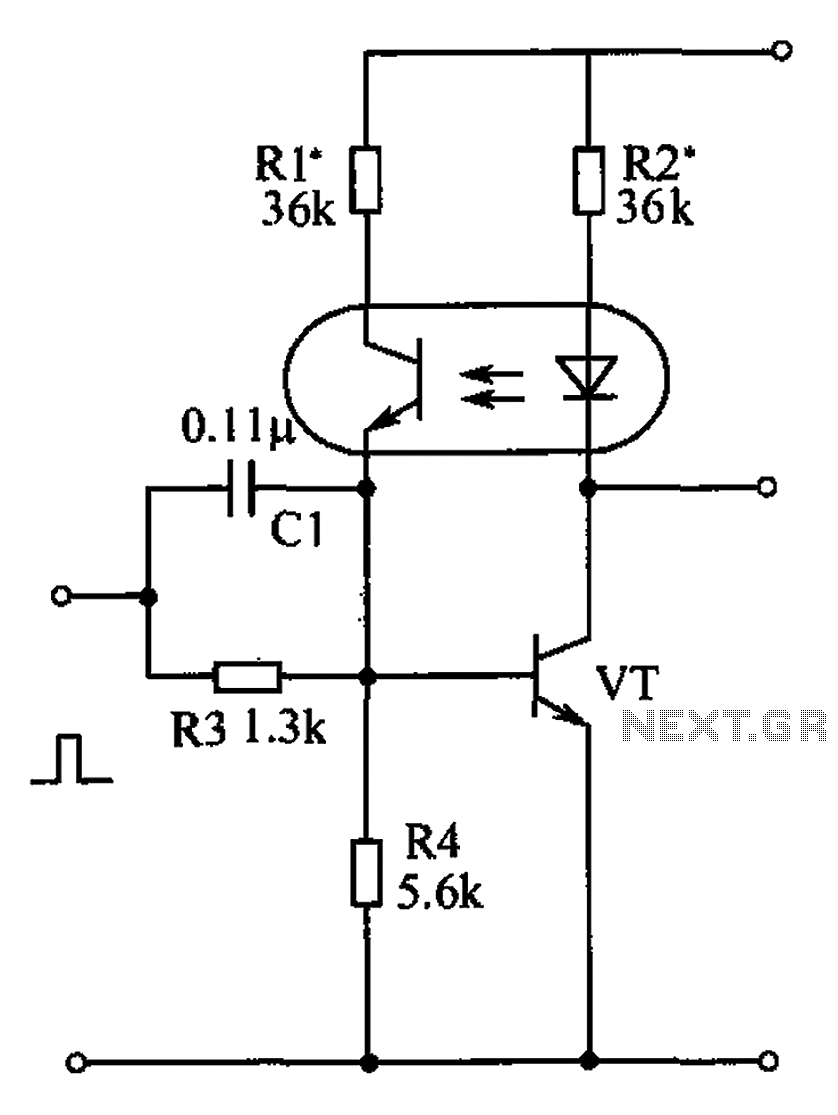
The bistable circuit and optocoupler transistor operate as illustrated in the accompanying figure. Initially, when the supply voltage is applied, the transistor VT is in the off state, resulting in a high output potential. Upon receiving a forward pulse...
The following circuit illustrates an Automatic Room Power Control Circuit Diagram. This circuit is based on the NE555 integrated circuit (IC). Features include the use of two Light Dependent Resistors (LDRs). The Automatic Room Power Control Circuit utilizes an NE555...
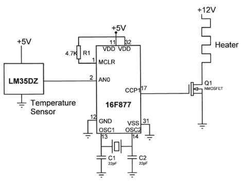
The electrical circuit diagram of this temperature control circuit consists of a 3-pin analog temperature sensor (LM35DZ), a built-in A/D converter microcontroller (PIC16F877), and the heater driver (IRL1004). The temperature control circuit utilizes the LM35DZ, a precision analog temperature sensor...
Warning: include(partials/cookie-banner.php): Failed to open stream: Permission denied in /var/www/html/nextgr/view-circuit.php on line 713
Warning: include(): Failed opening 'partials/cookie-banner.php' for inclusion (include_path='.:/usr/share/php') in /var/www/html/nextgr/view-circuit.php on line 713