
Audio DAC S / PDIF (AES3) to analog
 to analog")
The receiver is a phase coupling (PLL), which is required for proper function of the receiver and decoder. Output phase-Fitr hinge pin is connected to the eighth Voltage on this pin controls the internal oscillator (VCO). The voltage on this pin can therefore be assumed on the sampling frequency of the received signal. Another way to determine the sampling rate (if it were necessary), to measure frequency oscillator on pin 10 (RMCK). In developing the first version of the converter I used in the filter PLL component values from the datasheet (Crip = C3 = 2.2 nF CFILT = C4 = 47 nF and RFILT = R2 = 3 kOhm). Phase coupling, however, worked only for the sampling frequency (fs) 48 kHz. In order to work for 44.1 kHz, I shrunk the resistance R2 to 560 ohms. To calculate the filter can be found in [6].
The decoded data is taken from pin 18 guided (SDOUT) at the input of D/A. Clock the clock signal from pin 16 (OSCLK) receivers. Logic level signal on pin 17 (OLRCK) determines whether the data being transmitted to the left or right channel. The frequency of this signal corresponds to the audio sampling frequency (fs). For the operation D/A converter clock frequency is important (RMCK) on pin 10 of the receiver. It is actually the output of oscillator phase coupling. This frequency is governed by the D/A converter. Its stability depends on the uniformity of the samples the output signal (jitter). The ratio of frequency and RMCK OLRCK (FS) further specifies the number of times the signal in the D/A converter oversampled. This ratio can be arbitrary, circuit CS4334 accepts the Base-rate mode clock speed 256x, 384x and 512x CF. In this mode, the function of guaranteeing the sampling frequency (fs) 48 kHz. The sampling frequency of 96, respectively. 100 kHz transducer works in the high-rate mode, which is set the clock frequency of 128x and 192x CF. The problem is that the receiver hardware mode produces a clock speed 256x CF. Therefore, in direct communication with the D/A converter can be an audio sampling rate up to 48kHz. This limitation can be avoided involvement clock frequency divider between the two mA transmitter and receiver.
To reduce interference between signals are logic transmitter and receiver separated by resistors R8-R11. The analog signal at the output of the converter can cause the amplitude to 3.5 V. Above this reason, the filter is only implemented at the output RC article. I originally wanted to use a better higher order filters with operational amplifiers, but the current operational amplifiers (useful for audio) would require such a stress range greater than the supply voltage to 5 V. In contrast, the amplifier "rail-to-rail, which would signal amplitude 3, 5 V at 5 V supply voltage made no problems, not amplifying the acoustic signal is very appropriate. For ordinary purposes of the RC filter is completely meet.
The data sub-channel information bit U and C in serial form on wires 25 and 26 and the receiver clock signal OLRCK. The structure described is not used. In software mode circuit CS8415A this data can be read at once for the whole block. Some of the channel status bits are decoded and connected to separate terminals. The pin is a bit Copyright (indicate whether it is permitted to create a digital copy) to pin 3 preemphasis indication on pin 13 professional display mode, the pin 19 non-audio bit (indicates otherwise, as compressed data) and signal pin 28 indicates the original data.
The pin receiver 11 is a signal indicating the sum of various errors - the error rate, coding, or "fell" loop PLL. This signal is indicated by LEDs. Indicates virtually no or very distorted S/PDIF signal to the receiver is no longer able to handle. Then the output D/A converter can discover different noises. Therefore, in this case, the device disconnects the output from the converter and connects to the line input. Also, if it is set to a non-audio bit output is disconnected from the transmitter. RERR signals and non-AUDIO NOR gate are connected and routed through the connector K9 transistor T1, which gives the relay. Jumpers can be set to K9 permanently plugged converter, auto-switching converter and permanently disconnected. The first location is especially important in experiments with sound and animation. The second and third position of the jumper is advisable to replace the switch. They can easily compare our sound from the transmitter, for example, digitally connected to the CD player, sound from the analog output of that device.
Always connect the power supply voltage and reset the receiver. This is R4 and C5 connected to the outlet of the 9th At this point brings to use a resistor with resistance 1 Mohm (or more) and instead of expensive electrolytic capacitors use a cheap ceramic. Unfortunately, although the CMOS receiver circuit, flows at the level H to the reset input current of several microamperes. Resistor R4 must be small enough for entry level RST aroused H. In practice, it proved that they satisfy the resistor R4 100 Ohm. The relatively tough test my receiver several "stuck". So I added a button to the circuit SW1, which the receiver can be manually reset. Button, however, be omitted, the device can be reset by disconnecting and connecting the power supply.
In conclusion, the description should mention the power supply. In order to maximize the versatility to use just one power supply voltage. His relay powered directly and stabilizer 5 V minimum voltage stabilizer is used about 7 V. The relay was joined together up from 8.2 V. The minimum reserve therefore only a supply voltage of 9 V. The maximum voltage is limited by power loss stabilizer SMD. For higher voltage is necessary to use a standard stabilizer and relay coil for this higher voltage. The receiver needs a 5V power supply for analog circuit (input shaping and phase coupling) and voltage of 3-5 V (according to some parts of the catalog sheet 3 or 5 V). Voltage D/A Converter is also 5 V. Although we can supply all districts in a uniform supply voltage of 5 V is suitable power supply for digital part of the receiver to reduce - significantly reduces power consumption. Power supply for digital part is therefore reduced to about 3.5 mass involved in the diodes D1 and D2. In experiments with two independent sources showed that the supply voltage digital part is not critical - the receiver still worked at a voltage of 1.75 V. On the other hand, the analog power supply is critical. Although the data sheet shows both districts range from 4.5 to 5.5 V, the device stopped working when the voltage drops below 4.62 V. To reduce the noise power D/A Converter separated reactor. Supply voltage is applied to the soldering tip and the connector K2. He is sure D4 diode separated, because the network adapter can be connected to the output connector opposite polarity.
The mounting plate, I witnessed the following: The board will prepare a hole since all the connectors, so we can just plug into the board and solder. Then the jumpers and will be filled in the order of SMD resistors, capacitors and ICs. Finally, on the other parts will be filled by the board. Be careful when planting IO3 - is oriented in reverse than other ICs. Solder a piece of the choke plate to touch the foil. Shield layer of the conventional components are connected to the ground at the connector K1 or negative power supply voltage (0 V) supply wire soldered on both sides of the board. Do not forget to connect the ground at point X (in addition to C5) prostr?ením piece of wire and soldered on both sides of the board.
All the necessary connectors are on the board. Connectors J1 and K5 and K10 are breaking the pin rails. The K5 connector can connect another input signal connector S/PDIF receiver module with an optical or digital output from CD-ROM. Optical Receiver and CD-ROMs have outputs in TTL level, so that in this case, remove the jumper (jumper) J1. The K6 connectors (direct output DAC), K7 (output per relay) and K8 (line) can be connected as needed Cinch. If you do not need to have in the absence of a digital signal through the device, just put the K8 two jumpers, so this input is connected to the earth. Connector K4 neosazujeme. Involvement of the optical module is input to the Figure 5. The module used in optical receiver TORX173 (TORX176, TORX178) and voltage stabilizer. A special stabilizer is used primarily because SMD stabilizer in the transmitter is no longer a great power reserves and connecting the optical module should just "tighten". If you use the transmitter in a classical stabilizer 7805, or else the output voltage of 5 V, there is no reason to use it for power module TORX.
The output of optical modules can be connected to a connector K5 also need to disconnect J1. Due to the simplicity do not mention PCB. If necessary, the circuit can easily connect the universal piece of board. Because the circuit no longer produced CS8415A can not use a connection with him. After minor adjustments could be used later CS8416A circuit. This adjustment, however, I tried it and even then I do not plan to anytime soon. If you want to jump in yourself, you may be inspired engagement DAC Elektor magazine (November 2009, page 52). I'm not sure yet whether to engage the filter member at the outlet 8 - prefer to see data sheet. R1 75 ohm (82 ohm) D1 to D3 1N4148 SMD R2 4.7 Ohm (560 Ohm) D4 1N4001 SMD (or normal DO41) R3, R12 and R15, R20, R21 560 ohm T1 BC849C R4 100 kOhm IO1 CS8415A-CS R5 to R7 47 kOhm IO2 CS4334-KS R8-R11 47 ohm IO3 74HC02 (SMD) R16, R17 270 kOhm IO4 78L05 (SMD) R18, R19, R22 22 kohm LED1, LED2 LED 2mA red / red C1, C2 10 nF LED3, LED4 LED 2 mA, green / green C3 4.7 nF (2.2 nF) C4 150 nF (82 nF) Re1 RA12W-C (Takamisawa) or similar relay C5, C6, C7 2.2 In ?F/16 C8, C9 6.8 nF K1 cinch to PCB C10, C17 In 1910 ?F/16 K2 power outlet SCD-016 C11 to C16. 100 nF, ker K3, K4 3.5mm jack SCJ-0354 or EBS35 J1, K5 and K10 breakable connector strips L1 33 ?H, Choke axial SW1 the P-B1720C PCB BCS 40 BCS 41 SW2 two-position switch P-B143 Optical transmitter modules (TOTX. ..), receiver (TORX. ..) and fiber optic cables are quite expensive. Unsuccessfully, I pokuel for single PC and connect the amplifier "zbastlit" something cheaper. It turned out that the biggest problem is to devise a transmitter (it is sufficient even LED and resistor) or a receiver, but how could focus enough LED light into an optical fiber whose core has a diameter of only a fraction of a millimeter. The recovery is easy, the device has no setting elements and should work on first connection. The K9 mount LED RERR and we set jumper to position the DAC. Connect the regulated power supply and slowly we increase supply voltage from 0 to 12 volts should be current 40-60 mA, while pressing the reset button for about 20 to 30 mA. From the output (K3, K7) can hear the noise and various whistles. If everything is in order, bring the digital input signal and the output should appear in the decoded audio signal. Change any jumper from position to position the DAC car. Relay should now be switched on only when the input digital signal. Animated converter can build them into separate boxes, or into audio (pre) amplifiers, which will equip the digital input.
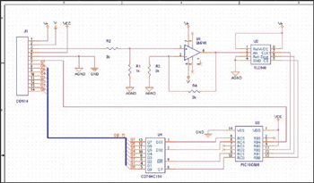
The converter is based on double circuit boards, staffed mostly SMT technology. All connections are kept on one side of the plate, on the other side is the area in the ground and five wire jumpers. Most components are SMD and are mounted on the circuit. On the other hand, boards are all connectors, relays, choke L1 and wire jumpers. LEDs, switch and reset button can be individually connected directly to the K9 connector, like the LEDs are connected to the PC motherboard. You can also use a board panel of Figure 4 transmitter to link it with the flat cable 16ilovým. The panel can also be connected permanently bent double row pin strip breaking. To convert the digital signal, there are a number of special districts, with differing complexity involved and the quality of the output signal. With these "easier" to build a single chip can interface with low power consumption and signal - noise 60-80 db. For larger signal to noise ratio should be separated from their own digital converter section. "Multi-chip" transducers achieve a distance from the noise of 120 dB, however, largely depends on proper design and printed circuit boards. All these districts are too fundamental flaw - in stores with electronic components is very bad and do not be shán?jíí. For the converter described here, I used circuits Crystal (The described device is used to convert the digital signal format S / PDIF (AES3) to analog. It can be used for any device with uncompressed digital audio output (desktop CD or DVD, minidisk, sound card PC CD-ROM). Separate transmitter can improve the signal to noise ratio and reduce noise, which is especially true for the PC sound card.
The device does not signal processor, and therefore not able to play back compressed or encoded multichannel signal (AC3, MP3, respectively. Mpeg)! The converter has been tested only for signals with a sampling frequency of 32 kHz (minidisc), 44.1 kHz (CD) and 48 kHz (sound card PC). For lower frequencies need to be adjusted PLL loop filter, the higher divider circuit to add two, see text.
Involvement of the transmitter to the receiver S / PDIF is the figure 1 . Digital input signal passes through C1 at the receiver input. Differential input receiver and the outlets RXP Rxn. The receiver is able to process signals from a few tens of millivolts for units of volts. Disconnect the jumper, J1, we can connect the input signal in TTL level, such as output from a CD-ROM or from the optical receiver. In hardware mode, the circuit is switched to the outlet level H 24th Resistors R5 and R7 is set circuit function.
Logic level on pin 3, 18 and 28 are read after a reset circuit, before they switched to the output pins. The receiver is a phase coupling (PLL), which is required for proper function of the receiver and decoder.
Output phase-Fitr hinge pin is connected to the eighth Voltage on this pin controls the internal oscillator (VCO). The voltage on this pin can therefore be assumed on the sampling frequency of the received signal. Another way to determine the sampling rate (if it were necessary), to measure frequency oscillator on pin 10 (RMCK).
In developing the first version of the converter I used in the filter PLL component values ??from the datasheet (Crip = C3 = = 2.2 nF CFILT = C4 = 47 nF and RFILT = R2 = 3 kOhm). Phase coupling, however, worked only for the sampling frequency (fs) 48 kHz. In order to work for 44.1 kHz, I shrunk the resistance R2 to 560 ohms. To calculate the filter can be found in [6]. The decoded data is taken from pin 18 guided (SDOUT) at the input of D / A. Clock the clock signal from pin 16 (OSCLK) receivers. Logic level signal on pin 17 (OLRCK) determines whether the data being transmitted to the left or right channel.
The frequency of this signal corresponds to the audio sampling frequency (fs). For the operation D / A converter clock frequency is important (RMCK) on pin 10 of the receiver. It is actually the output of oscillator phase coupling. This frequency is governed by the D / A converter. Its stability depends on the uniformity of the samples the output signal (jitter). The ratio of frequency and RMCK OLRCK (FS) further specifies the number of times the signal in the D / A converter oversampled. This ratio can be arbitrary, circuit CS4334 accepts the Base-rate mode clock speed 256x, 384x and 512x CF.
In this mode, the function of guaranteeing the sampling frequency (fs) 48 kHz. The sampling frequency of 96, respectively. 100 kHz transducer works in the high-rate mode, which is set the clock frequency of 128x and 192x CF. The problem is that the receiver hardware mode produces a clock speed 256x CF. Therefore, in direct communication with the D / A converter can be an audio sampling rate up to 48kHz.
This limitation can be avoided involvement clock frequency divider between the two mA transmitter and receiver. To reduce interference between signals are logic transmitter and receiver separated by resistors R8-R11.
The analog signal at the output of the converter can cause the amplitude to 3.5 V. Above this reason, the filter is only implemented at the output RC article. I originally wanted to use a better higher order filters with operational amplifiers, but the current operational amplifiers (useful for audio) would require such a stress range greater than the supply voltage to 5 V. In contrast, the amplifier "rail-to-rail, which would signal amplitude 3 , 5 V at 5 V supply voltage made no problems, not amplifying the acoustic signal is very appropriate.
For ordinary purposes of the RC filter is completely meet. The data sub-channel information bit U and C in serial form on wires 25 and 26 and the receiver clock signal OLRCK. The structure described is not used. In software mode circuit CS8415A this data can be read at once for the whole block. Some of the channel status bits are decoded and connected to separate terminals. The pin is a bit Copyright (indicate whether it is permitted to create a digital copy) to pin 3 preemphasis indication on pin 13 professional display mode, the pin 19 non-audio bit (indicates otherwise, as compressed data) and signal pin 28 indicates the original data.
The pin receiver 11 is a signal indicating the sum of various errors - the error rate, coding, or "fell" loop PLL. This signal is indicated by LEDs. Indicates virtually no or very distorted S / PDIF signal to the receiver is no longer able to handle.
Then the output D / A converter can discover different noises. Therefore, in this case, the device disconnects the output from the converter and connects to the line input. Also, if it is set to a non-audio bit output is disconnected from the transmitter. RERR signals and non-AUDIO NOR gate are connected and routed through the connector K9 transistor T1, which gives the relay.
Jumpers can be set to K9 permanently plugged converter, auto-switching converter and permanently disconnected. The first location is especially important in experiments with sound and animation. The second and third position of the jumper is advisable to replace the switch. They can easily compare our sound from the transmitter, for example, digitally connected to the CD player, sound from the analog output of that device.
Always connect the power supply voltage and reset the receiver. This is R4 and C5 connected to the outlet of the 9th At this point brings to use a resistor with resistance 1 Mohm (or more) and instead of expensive electrolytic capacitors use a cheap ceramic. Unfortunately, although the CMOS receiver circuit, flows at the level H to the reset input current of several microamperes.
Resistor R4 must be small enough for entry level RST aroused H. In practice, it proved that they satisfy the resistor R4 100 Ohm. The relatively tough test my receiver several "stuck". So I added a button to the circuit SW1, which the receiver can be manually reset. Button, however, be omitted, the device can be reset by disconnecting and connecting the power supply. In conclusion, the description should mention the power supply. In order to maximize the versatility to use just one power supply voltage. His relay powered directly and stabilizer 5 V minimum voltage stabilizer is used about 7 V. The relay was joined together up from 8.2 V. The minimum reserve therefore only a supply voltage of 9 V. The maximum voltage is limited by power loss stabilizer SMD. For higher voltage is necessary to use a standard stabilizer and relay coil for this higher voltage. The receiver needs a 5V power supply for analog circuit (input shaping and phase coupling) and voltage of 3-5 V (according to some parts of the catalog sheet 3 or 5 V).
Voltage D / A Converter is also 5 V. Although we can supply all districts in a uniform supply voltage of 5 V is suitable power supply for digital part of the receiver to reduce - significantly reduces power consumption. Power supply for digital part is therefore reduced to about 3.5 mass involved in the diodes D1 and D2.
In experiments with two independent sources showed that the supply voltage digital part is not critical - the receiver still worked at a voltage of 1.75 V. On the other hand, the analog power supply is critical. Although the data sheet shows both districts range from 4.5 to 5.5 V, the device stopped working when the voltage drops below 4.62 V.
To reduce the noise power D / A Converter separated reactor. Supply voltage is applied to the soldering tip and the connector K2. He is sure D4 diode separated, because the network adapter can be connected to the output connector opposite polarity. The mounting plate, I witnessed the following: The board will prepare a hole since all the connectors, so we can just plug into the board and solder.
Then the jumpers and will be filled in the order of SMD resistors, capacitors and ICs. Finally, on the other parts will be filled by the board. Be careful when planting IO3 - is oriented in reverse than other ICs. Solder a piece of the choke plate to touch the foil. Shield layer of the conventional components are connected to the ground at the connector K1 or negative power supply voltage (0 V) supply wire soldered on both sides of the board. Do not forget to connect the ground at point X (in addition to C5) prostr?ením piece of wire and soldered on both sides of the board.
All the necessary connectors are on the board. Connectors J1 and K5 and K10 are breaking the pin rails. The K5 connector can connect another input signal connector S / PDIF receiver module with an optical or digital output from CD-ROM. Optical Receiver and CD-ROMs have outputs in TTL level, so that in this case, remove the jumper (jumper) J1.
The K6 connectors (direct output DAC), K7 (output per relay) and K8 (line) can be connected as needed Cinch. If you do not need to have in the absence of a digital signal through the device, just put the K8 two jumpers, so this input is connected to the earth.
Connector K4 neosazujeme. Involvement of the optical module is input to the Figure 5 . The module used in optical receiver TORX173 (TORX176, TORX178) and voltage stabilizer. A special stabilizer is used primarily because SMD stabilizer in the transmitter is no longer a great power reserves and connecting the optical module should just "tighten". If you use the transmitter in a classical stabilizer 7805, or else the output voltage of 5 V, there is no reason to use it for power module TORX.
The output of optical modules can be connected to a connector K5 also need to disconnect J1. Due to the simplicity do not mention PCB. If necessary, the circuit can easily connect the universal piece of board. Because the circuit no longer produced CS8415A can not use a connection with him. After minor adjustments could be used later CS8416A circuit. This adjustment, however, I tried it and even then I do not plan to anytime soon. If you want to jump in yourself, you may be inspired engagement DAC Elektor magazine (November 2009, page 52). I'm not sure yet whether to engage the filter member at the outlet 8 - prefer to see data sheet. R1 75 ohm (82 ohm) D1 to D3 1N4148 SMD R2 4.7 Ohm ( 560 Ohm ) D4 1N4001 SMD (or normal DO41) R3, R12 and R15, R20, R21 560 ohm T1 BC849C R4 100 kOhm IO1 CS8415A-CS R5 to R7 47 kOhm IO2 CS4334-KS R8-R11 47 ohm IO3 74HC02 (SMD) R16, R17 270 kOhm IO4 78L05 (SMD) R18, R19, R22 22 kohm LED1, LED2 LED 2mA red / red C1, C2 10 nF LED3, LED4 LED 2 mA, green / green C3 4.7 nF ( 2.2 nF ) C4 150 nF ( 82 nF ) Re1 RA12W-C (Takamisawa) or similar relay C5, C6, C7 2.2 In ?F/16 C8, C9 6.8 nF K1 cinch to PCB C10, C17 In 1910 ?F/16 K2 power outlet SCD-016 C11 to C16.
100 nF, ker K3, K4 3.5mm jack SCJ-0354 or EBS35 J1, K5 and K10 breakable connector strips L1 33 ?H, Choke axial SW1 the P-B1720C PCB BCS 40 BCS 41 SW2 two-position switch P-B143 Optical transmitter modules (TOTX. ..), receiver (TORX. ..) and fiber optic cables are quite expensive. Unsuccessfully, I pokuel for single PC and connect the amplifier "zbastlit" something cheaper. It turned out that the biggest problem is to devise a transmitter (it is sufficient even LED and resistor) or a receiver, but how could focus enough LED light into an optical fiber whose core has a diameter of only a fraction of a millimeter.
The recovery is easy, the device has no setting elements and should work on first connection. The K9 mount LED RERR and we set jumper to position the DAC. Connect the regulated power supply and slowly we increase supply voltage from 0 to 12 volts should be current 40-60 mA, while pressing the reset button for about 20 to 30 mA. From the output (K3, K7) can hear the noise and various whistles. If everything is in order, bring the digital input signal and the output should appear in the decoded audio signal.
Change any jumper from position to position the DAC car. Relay should now be switched on only when the input digital signal. Animated converter can build them into separate boxes, or into audio (pre) amplifiers, which will equip the digital input. The converter is based on double circuit boards, staffed mostly SMT technology. All connections are kept on one side of the plate, on the other side is the area in the ground and five wire jumpers.
Most components are SMD and are mounted on the circuit. On the other hand, boards are all connectors, relays, choke L1 and wire jumpers. LEDs, switch and reset button can be individually connected directly to the K9 connector, like the LEDs are connected to the PC motherboard. You can also use a board panel of Figure 4 transmitter to link it with the flat cable 16ilovým. The panel can also be connected permanently bent double row pin strip breaking. To convert the digital signal, there are a number of special districts, with differing complexity involved and the quality of the output signal.
With these "easier" to build a single chip can interface with low power consumption and signal - noise 60-80 db. For larger signal to noise ratio should be separated from their own digital converter section. "Multi-chip" transducers achieve a distance from the noise of 120 dB, however, largely depends on proper design and printed circuit boards.
All these districts are too fundamental flaw - in stores with electronic components is very bad and do not be shán?jíí. For the converter described here, I used circuits Crystal (Cirrus Logic), which can be purchased from HT EUREP ( www.hte.cz ).
The core of the converter consists of two districts - receiver decoder and an S / PDIF (or AES3) and custom converter D / A. Receiver S / PDIF CS8415A is a very interesting district. According to the logic levels on input H / S can work in two entirely different modes. If you select the software mode, you have the power (reset) circuit program first set. The receiver will have 7 inputs, which can switch software, and registers can be read by all possible sub-channel information that is contained in the input signal.
Interface circuit for various ways to connect the control of microcontroller and multiple formats of output data. If you select the hardware mode, you do not need a microprocessor, but some of the features you need to resign.
Almost half of the terminals and the circuit changes the meaning of the required circuit function is set pull-ups and pull-down resistors on three outlets. (Ie a resistor, connected from pin to supply voltage or ground.) Subset of the features available in hardware mode is selected very efficiently, and if we do not need access to the registry district, or change the settings or continuous function circuit, microprocessor control, without the bypass.
Details can be found in a comprehensive data sheet [2]. Converter is described in the hardware mode circuit. D / A converter CS4334 uses the default mode eightfold oversampling the input signal. Reduces noise and thus greatly simplifies the particular output filter, which is already partially integrated. The sigma-delta converter circuit is connected digital and analog filter. For general purposes it is enough to output a simple circuit involving a member of the RC. 🔗 External reference
Related Circuits
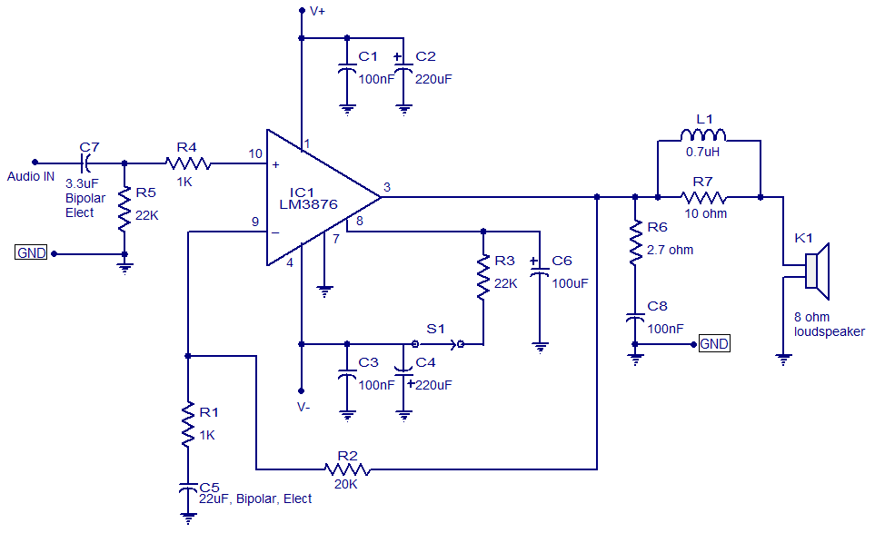
LM3876-based 50-watt audio amplifier circuit. Operates from +/-35V DC. Simple design, low noise. The LM3876 is a high-performance audio power amplifier designed for driving speakers in various audio applications. This particular circuit configuration enables the amplifier to deliver up to...
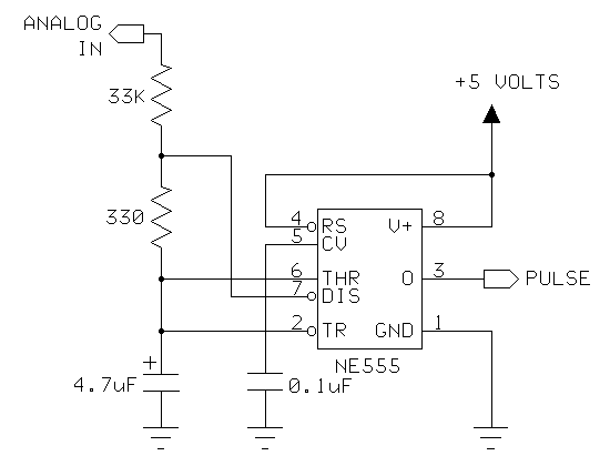
This circuit, based on the 555 timer, functions as a voltmeter and an analog-to-digital converter, converting analog input voltage into digital output pulses. The 555 timer is a versatile integrated circuit commonly used for timing, oscillation, and pulse generation applications....
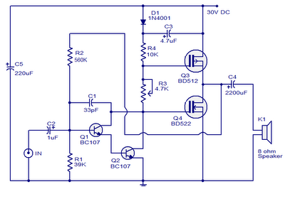
This is a 10W MOSFET audio amplifier circuit that operates from a single power source. Single rail configurations are seldom used in Class B power amplifiers; however, they are suitable for low-power applications like this one. This circuit design...
The following application circuits are designed to demonstrate several key concepts: A 2 kΩ resistor should be placed in series with the voltage source to limit supply current and mitigate negative ringing on the bit inputs. Temperature compensation for...
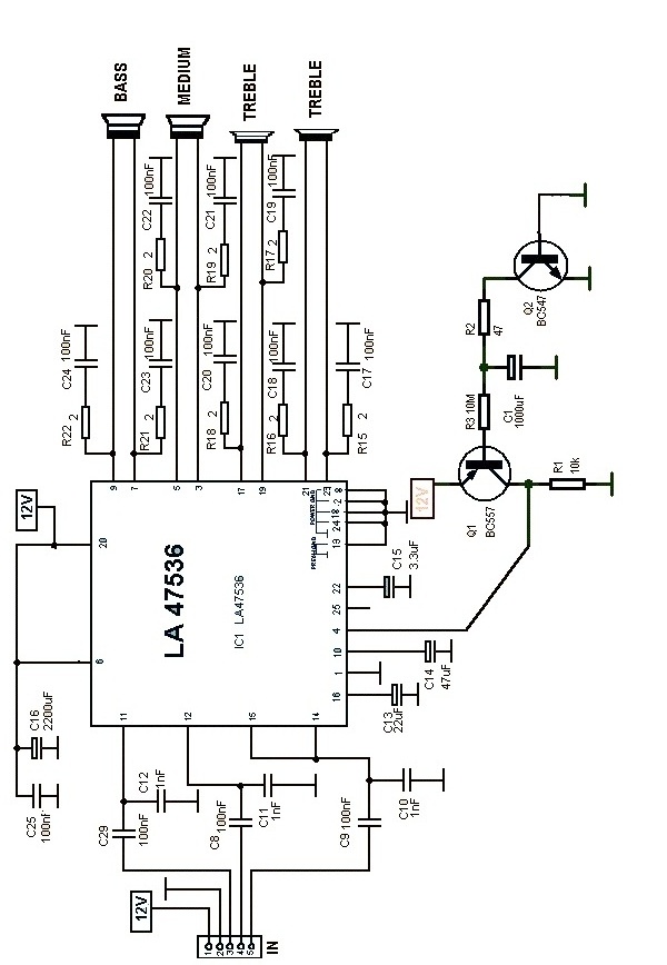
This car audio amplifier circuit is based on the LA47536 audio amplifier integrated circuit designed by Sanyo. This audio amplifier circuit is specifically designed for car audio power amplifiers. The LA47536 car audio amplifier IC features four output channels...
This example demonstrates the design of a circuit that incorporates both analog and digital components, features multiple power planes, and utilizes a single ground plane that is divided into analog and digital sections while maintaining a common reference point. The...