
Automatic-shutoff
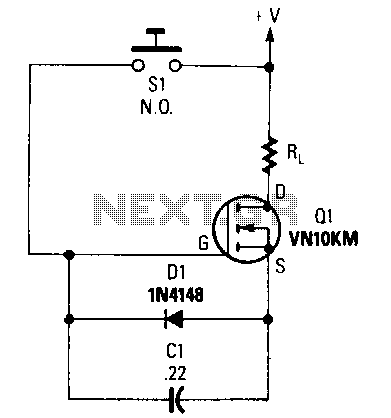
When switch S1 is pressed, capacitor C1 begins to charge to the supply voltage. This action creates a forward bias on the gate of transistor Q1, turning it on and allowing current to flow to the load resistor RL. As the charge on capacitor C1 dissipates, the transistor turns off, interrupting the current supply to the load. The load can be a variety of devices, such as a transistor radio or a child's toy. Transistor Q1 is rated for 0.5 A at 60 V DC. With a supply voltage of 9 V DC and capacitor C1 rated at 0.22 µF, a delay of approximately one minute is produced; using a capacitor rated at 10 µF results in a delay of about one hour.
The circuit operates as a simple timing mechanism utilizing a capacitor and a transistor switch. When switch S1 is engaged, the capacitor C1 charges through the supply voltage, which is set at 9 V DC. The charging process allows the voltage across C1 to rise, eventually exceeding the threshold voltage necessary to forward-bias the gate of transistor Q1. This action activates Q1, enabling it to conduct and supply current to the load resistor RL.
The load resistor RL is critical as it determines the current flowing through the connected load, which can be any device that operates within the specifications of the circuit. The choice of transistor Q1 is essential, as it must handle the load current without exceeding its maximum ratings. With a maximum current rating of 0.5 A and a voltage rating of 60 V DC, Q1 is suitable for low-power applications.
As the capacitor C1 discharges through the load when Q1 is activated, it gradually loses its stored charge. Once the voltage across C1 drops below the necessary threshold to keep Q1 in the 'on' state, the transistor will turn off, ceasing current flow to the load. The timing of this process is primarily influenced by the capacitance value of C1. A capacitor rated at 0.22 µF provides a delay of approximately one minute, while a larger capacitor, rated at 10 µF, extends the delay to about one hour. This characteristic allows for flexibility in designing circuits that require specific timing intervals based on the application needs.
Overall, this circuit exemplifies a straightforward approach to creating a timed control mechanism using basic electronic components, with applications ranging from simple toys to more complex electronic devices.When Sl is depressed, Cl begins to charge to the supply voltage. That places a forward bias on the gate of Ql turning it on and supplying current to load resistor RL. When the charge on Clleaks off, the transistor shuts off, cutting off current to the load. That load could be anything from a transistor radio to a child"s toy. Transistor Ql, is rated at 0.5 A at 60 V de. With a supply voltage of 9 V de and with Cl rated at 0.22 J🔗 External reference
The circuit operates as a simple timing mechanism utilizing a capacitor and a transistor switch. When switch S1 is engaged, the capacitor C1 charges through the supply voltage, which is set at 9 V DC. The charging process allows the voltage across C1 to rise, eventually exceeding the threshold voltage necessary to forward-bias the gate of transistor Q1. This action activates Q1, enabling it to conduct and supply current to the load resistor RL.
The load resistor RL is critical as it determines the current flowing through the connected load, which can be any device that operates within the specifications of the circuit. The choice of transistor Q1 is essential, as it must handle the load current without exceeding its maximum ratings. With a maximum current rating of 0.5 A and a voltage rating of 60 V DC, Q1 is suitable for low-power applications.
As the capacitor C1 discharges through the load when Q1 is activated, it gradually loses its stored charge. Once the voltage across C1 drops below the necessary threshold to keep Q1 in the 'on' state, the transistor will turn off, ceasing current flow to the load. The timing of this process is primarily influenced by the capacitance value of C1. A capacitor rated at 0.22 µF provides a delay of approximately one minute, while a larger capacitor, rated at 10 µF, extends the delay to about one hour. This characteristic allows for flexibility in designing circuits that require specific timing intervals based on the application needs.
Overall, this circuit exemplifies a straightforward approach to creating a timed control mechanism using basic electronic components, with applications ranging from simple toys to more complex electronic devices.When Sl is depressed, Cl begins to charge to the supply voltage. That places a forward bias on the gate of Ql turning it on and supplying current to load resistor RL. When the charge on Clleaks off, the transistor shuts off, cutting off current to the load. That load could be anything from a transistor radio to a child"s toy. Transistor Ql, is rated at 0.5 A at 60 V de. With a supply voltage of 9 V de and with Cl rated at 0.22 J