
Balanced-modulator

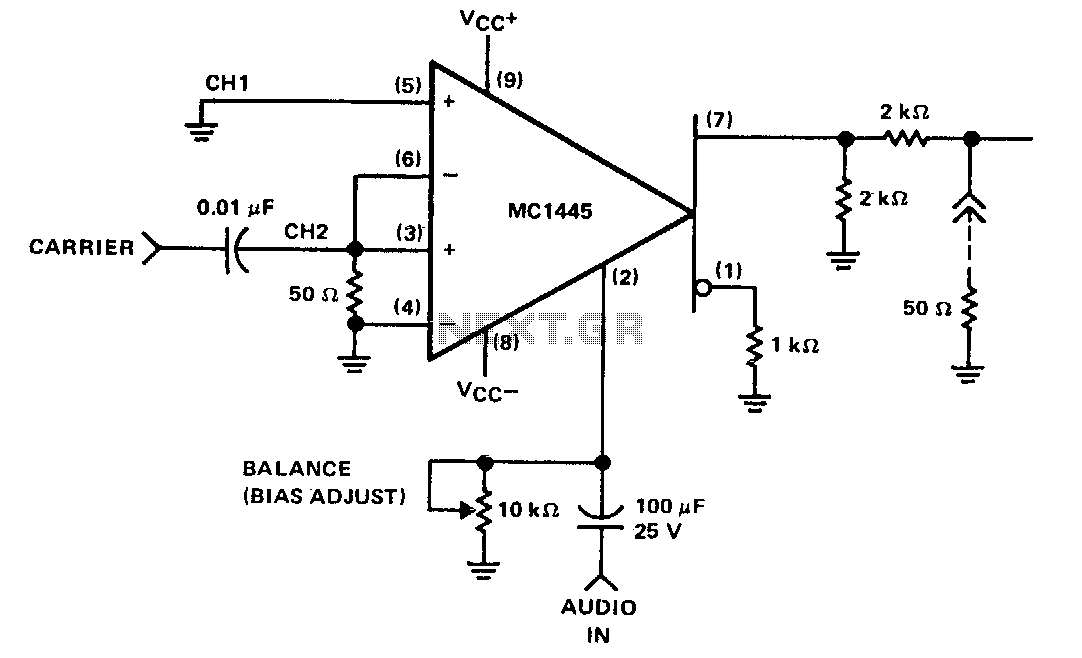
This circuit transmits the input signal at unity gain, either in its original form or inverted, based on the digital control input. A buffered input is utilized, as low source impedance is crucial. Gain can be introduced through modifications to the feedback networks. The circuit can handle signals up to 100 kHz with a peak-to-peak output of 20.0 V. When the digital control input is driven by a reference phase that matches the frequency of the input signal, the circuit operates as a phase detector. The average direct current output is proportional to the phase difference, reaching 0 V at +90 degrees. By linking the output to a comparator, which subsequently drives the digital control, a synchronous full-wave rectifier is created. With a low-frequency input signal and a high-frequency digital control signal, a balanced modulator with suppressed carrier is formed.
This circuit employs a configuration that utilizes a buffered input stage to ensure low output impedance, which is critical for maintaining signal integrity and minimizing distortion. The unity gain characteristic allows for direct signal transmission without amplification or attenuation, ensuring that the signal remains faithful to its original characteristics. The circuit's ability to switch between unchanged and inverted outputs is governed by a digital control input, facilitating versatile signal processing applications.
The feedback network can be tailored to introduce gain, allowing the circuit to amplify the input signal as needed. This adaptability makes the circuit suitable for a variety of applications where signal conditioning is required. The operational bandwidth of 100 kHz is adequate for many audio and control signal applications, while the specified peak-to-peak output voltage of 20.0 V indicates robustness in handling larger signal amplitudes.
In phase detection applications, the circuit's performance is enhanced when the digital control input is synchronized with the frequency of the input signal. The resulting average direct current output provides a measure of the phase difference between the two signals, enabling precise phase measurement capabilities. The 0 V output at +90 degrees signifies a critical point where the input and reference signals are perfectly out of phase, a useful feature in various control systems.
The integration of a comparator at the output stage allows for the creation of a synchronous full-wave rectifier, which is advantageous for converting alternating current signals into direct current with reduced ripple. This configuration is particularly beneficial in power supply applications where efficient rectification is necessary.
Furthermore, the circuit's design accommodates the simultaneous processing of low-frequency input signals and high-frequency digital control signals, resulting in a balanced modulator. This capability is essential for applications in communication systems where carrier suppression is required to enhance signal quality and reduce interference. Overall, this circuit presents a versatile solution for various electronic signal processing needs, combining phase detection, rectification, and modulation functionalities in a single design.This circuit passes the input signal at unity gain, either unchanged or inverted, depending on the digital control input. A buffered input is shown, since low-source impedance is essential. Gain can be added by modifications to the feedback networks. Signals up to 100kHz can be handled with 20.0-V pk-pk, output. The circuit becomes a phase detector when driving the digital control input with a reference phase at the same frequency as the input signal;
the average de output is proportional to the phase difference, with 0 V at + 90°. By connecting the output to a comparator, which in tum drives the digital control, a synchronous full-wave rectifier is formed. With a low-frequency input signal and a high-frequency digital control signal, a balanced (suppressed carrier) modulator is formed.
Related Circuits
When the carrier level is sufficient to activate the cross-coupled pair of differential amplifiers, the modulation signal applied to the gate will be switched at the carrier frequency between the collector loads. This switching results in the modulation being...