
Battery Powered One-Time-Only Alarm - Support Material
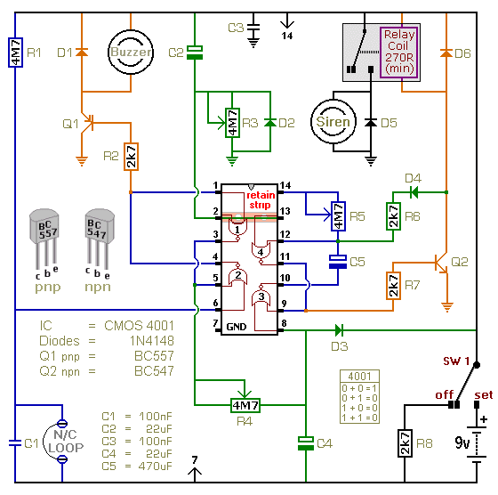
In standby mode, the normally closed loop connects pin 6 to ground, diverting current through resistor R1 to ground as well. When the door is opened, the loop is interrupted, causing R1 to quickly charge capacitor C1, which raises the voltage at pin 6. This high voltage at one of the inputs of gate 2 causes the output at pin 4 to go low. Consequently, current flows through the emitter-base junction of transistor Q1 and resistor R2 into pin 4, turning on Q1. This action connects the negative terminal of the buzzer to ground, activating it.
Pin 4 is linked to pin 1, so when pin 4 goes low, pin 1 also goes low. Since R3 is already holding pin 2 low, the low state of pin 1 causes the output at pin 3 of gate 1 to go high. This high output serves two functions: it latches itself on and initiates the entry delay timer. To ensure that pin 3 remains high even after the door is closed and the loop is restored, it must latch itself on by driving pin 5 high.
For pin 3 to maintain a high state, pin 1 must remain low, which in turn requires pin 4 to be low. To keep pin 4 low, at least one input of gate 2 must remain high. When pin 3 goes high, it drives pin 5 high, ensuring that pin 1 stays low and pin 3 remains high. This self-latching mechanism allows pin 3 to maintain its state regardless of whether the loop is open or closed.
The second function of pin 3 is to charge capacitor C4 through resistor R4. While pin 3 is low, it keeps pin 8 low via R4, ensuring that C4 remains discharged. Once pin 3 transitions high, it begins to charge C4 slowly through R4, initiating the entry delay. Depending on the value of R4, this entry delay can last up to approximately 60 seconds or more. During this time, the user typically moves switch SW1 to the off position. If this action is not taken, when the voltage across C4 reaches a predetermined threshold, it will trigger additional actions in the circuit, potentially leading to alarm activation or other predefined responses.The Cmos 4001 has four - independent - two-input NOR gates. The four gates are divided into two pairs. Gates 1 & 2 are wired together to form a type of latching circuit. When the alarm is triggered - they will latch - and sound the buzzer. Gates 3 & 4 are wired to form a monostable. When the entry delay expires - the monostable will sound the sire n for a fixed length of time. Then the siren will switch off - and stay off. = Cmos 4001 gates only have a high output when both inputs are low. See the truth table. When you switch the alarm on - C2 is in a discharged state. Because it`s discharged - the capacitor acts like a wire link connecting pins 2 & 13 to the positive line. This means that gates 1 & 4 each have one high input. These high inputs - force the output pins of gates 1 & 4 to remain low. And while the output pins of gates 1 & 4 are forced to remain low - both the latching circuit and the monostable are disabled.
In other words - the alarm cannot be activated. = C2 will continue to hold pins 2 & 13 high - until it charges through R3. This is the exit delay. Depending on the setting of R3 - it will last for up to a minute or more. During this period - you may open the loop and leave the building without activating the alarm. = As C2 charges - the voltage on the negative terminal of the capacitor falls. When it falls to just below half the supply voltage - it takes pins 2 & 13 low. When pins 2 & 13 go low - the outputs of gates 1 & 4 are no longer forced to remain low. This means that both the latch and the monostable circuits are enabled. In other words - the exit delay is over - and it`s now possible to activate the alarm. = In standby mode - the normally closed loop connects pin 6 to ground. And the current through R1 is also diverted to ground through the loop. When you return and open the door - the loop is broken. R1 quickly charges C1 - and the voltage on the capacitor takes pin 6 high. = Because one of the gate 2 inputs goes high - its output at pin 4 will go low. See the truth table. When pin 4 goes low - current flows through the emitter-base junction of Q1 and R2 - into pin 4. This switches Q1 on. The transistor connects the negative lead of the buzzer to ground - and the buzzer sounds. = Pin 4 is connected to pin 1. So when pin 4 goes low - it takes pin 1 low. You`ll recall that R3 is already holding pin 2 low So when pin 1 goes low - the gate 1 output at pin 3 goes high. See the truth table. When pin 3 goes high - it does two different jobs. It latches itself on - and it starts the entry delay timer. = We want pin 3 to remain high - even after the door has been closed and the loop restored. Otherwise you could defeat the alarm by simply closing the door behind you. So pin 3 must latch itself on. It does this by taking pin 5 high. = For pin 3 to remain high - pin 1 must remain low. For pin 1 to remain low - pin 4 must remain low. For pin 4 to remain low - at least one of the gate 2 inputs must remain high. See the truth table. = Pin 3 is connected to pin 5. When pin 3 goes high - it takes pin 5 high. So pin 3 is holding one of the gate 2 inputs high. While at least one of the gate 2 inputs is high - pin 4 will remain low. And while pin 4 holds pin 1 low - pin 3 will remain high. = In other words - pin 3 has latched itself on. It no longer needs R1 to hold pin 6 high. Because pin 3 is holding pin 5 high - pin 1 will remain low - and pin 3 will remain high. It makes no difference now whether the loop is open or closed. = Pin 3`s second job is to charge C4 through R4. While pin 3 is low - it holds pin 8 low through R4. It also keeps C4 discharged. = When pin 3 goes high - it begins to charge C4 slowly - through R4. This is the entry delay. Depending on the setting of R4 - the entry delay will last for up to about 60-seconds or more. During this time - you will normally move Sw1 to the off position. If you fail to do so - when the voltage on C4 reach 🔗 External reference
Related Circuits

When the SI (sensor) is closed, power is applied to U2, a dual timer. After a time determined by C2, CI is energized after a predetermined time determined by the value of C5. Pin 9 of U2 becomes low,...
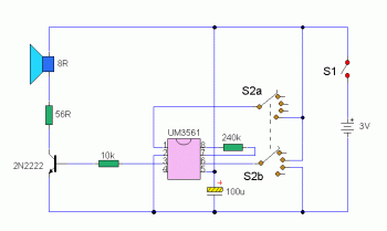
This schematic is simple and easy to construct. The integrated circuit (IC) generates all the sound effects, with the output at Pin 3 being amplified by a transistor. A 64-ohm loudspeaker can be used instead of the 56-ohm resistor...
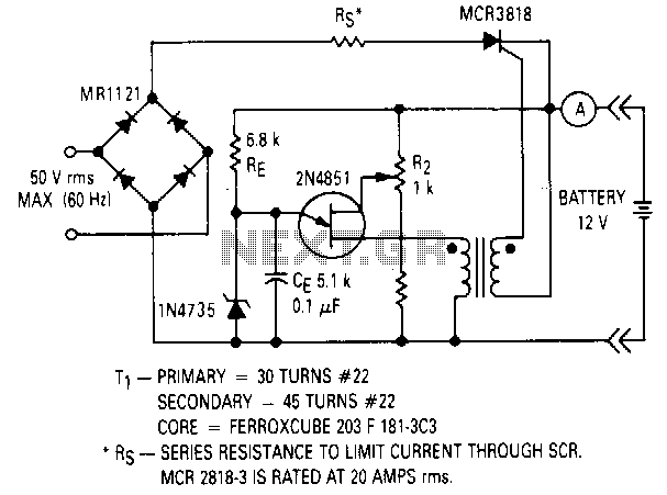
This circuit will not function unless the battery to be charged is connected with the correct polarity. The voltage of the battery regulates the charger, and when the battery is fully charged, the charger will stop supplying current to...
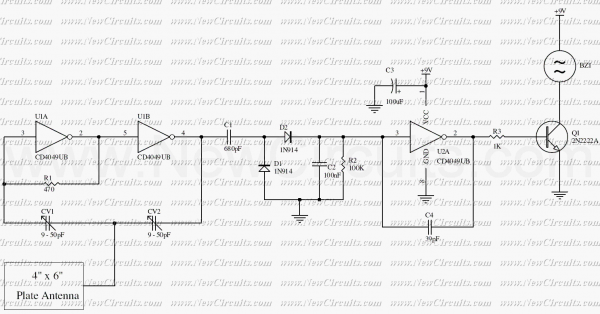
Inverters U1a and U1b are connected in a simple RC oscillator circuit. The frequency is determined by the values of R1, C1, C2 and the internal characteristics of the integrated circuit. As long as the circuit is oscillating, a...
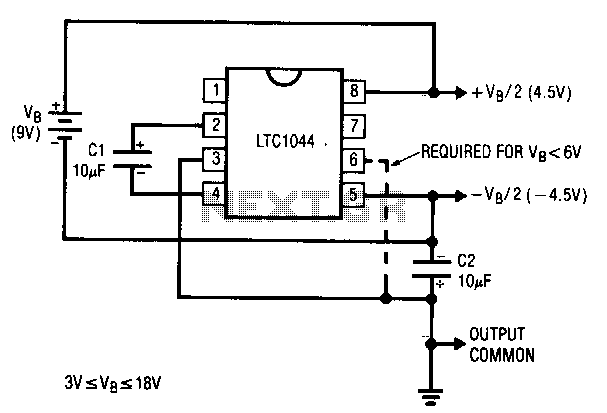
A common requirement in many systems is to obtain both positive and negative supplies from a single battery. For applications with small current needs, the circuit illustrated provides a straightforward solution. It generates symmetrical output voltages of ±, each...
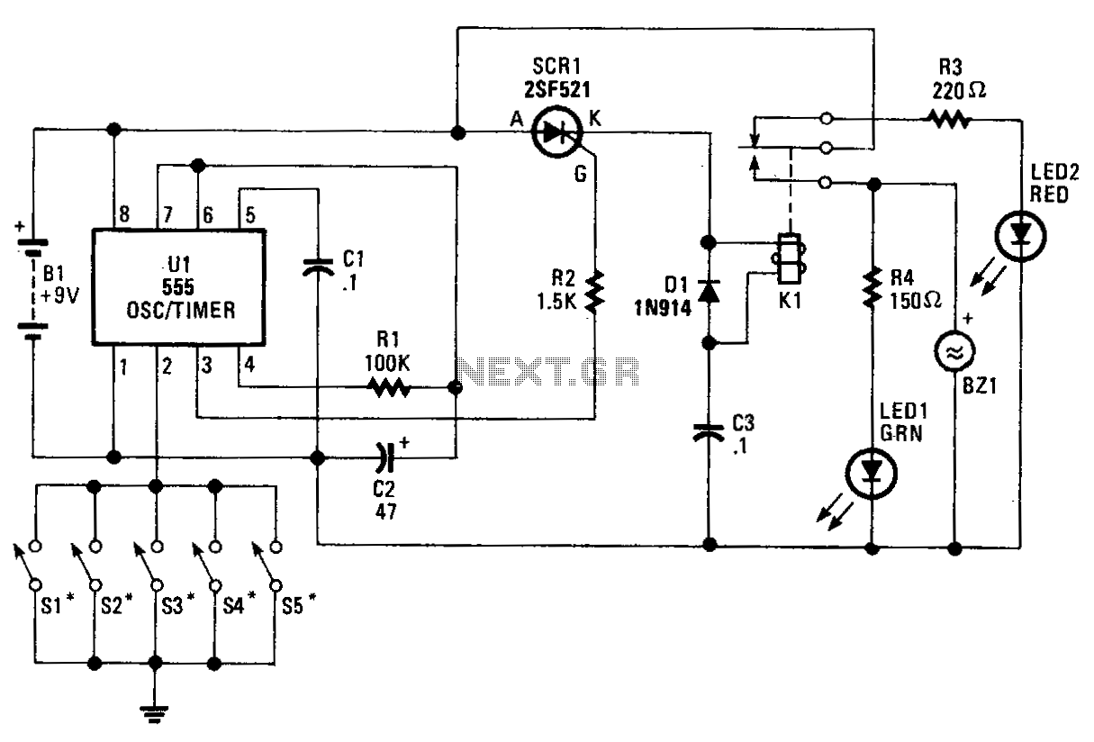
The core component of the circuit is a 555 timer/oscillator, designated as U1, which is configured for monostable operation. The output from U1 at pin 3 is connected to the gate of SCR1. As long as switches S1 to...
Warning: include(partials/cookie-banner.php): Failed to open stream: Permission denied in /var/www/html/nextgr/view-circuit.php on line 713
Warning: include(): Failed opening 'partials/cookie-banner.php' for inclusion (include_path='.:/usr/share/php') in /var/www/html/nextgr/view-circuit.php on line 713