
bidirectional power inverter
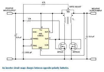
The symmetrical flyback converter serves as an efficient solution for managing energy transfer between two battery buses with differing charge levels. The circuit's design allows for flexibility in output voltage, making it suitable for various applications where voltage levels may need to be adjusted dynamically. The use of synchronous switching enhances the converter's efficiency, particularly in scenarios where the output voltage closely matches the desired levels.
The incorporation of a comparator to regulate the switching ratio is a critical feature that ensures the charge flows in the preferred direction, thus optimizing battery usage and prolonging battery life. This automatic charge replacement mechanism is especially useful in energy-sensitive applications, where maintaining battery health is paramount.
The design considerations for minimizing losses include selecting FETs with lower gate capacitance, which reduces the energy required for switching operations. This can significantly enhance overall efficiency, particularly in high-frequency applications where switching losses are more pronounced. Furthermore, the option to deactivate both FETs when battery voltages are balanced prevents unnecessary energy consumption, thus contributing to the longevity of the circuit's operation.
The voltage ratings associated with the components, such as the ±9V limit of the CMOS 555 timer, are crucial for ensuring the reliability and safety of the circuit. Operating within these voltage limits is essential to prevent component failure and maintain circuit integrity. The ability to supply approximately 100 mA makes this prototype suitable for a wide range of low to moderate power applications, effectively addressing the needs of systems reliant on battery power management.To swap charge in either direction between unevenly loaded positive and negative battery buses, you need an inverting dc transformer. One implementation is the symmetrical flyback converter shown in Figure 1. The circuit can generate a negative output from a positive supply or a positive output from a negative supply.
When the circuitstarts up, the substrate diode of the output FET bootstraps the output voltage to the point where synchronous switching takes over. When the gate-switching signal is symmetrical, the output voltage is approximately -95% of the input voltage, and the efficiency is greater than 80%. You can obtain voltage step-up or step-down by adjusting the switching ratio. When I used the circuit between two 4V lead-acid batteries, a comparator adjusted the switch ratio to drive charge in the desired direction.
The circuit automatically replaces charge drained from one battery to the other. In a short-battery-life application, the 2. 5-mA standby current from each battery may be negligible. Using lower-gate-capacitance, FETs can reduce losses. Alternatively, you can add gates to the drive circuit to turn off both FETs whenever the battery voltages balance. The minimum input voltage is a function of the gate thresholds of the FETs. The ±9V rating of the CMOS 555 timer sets the maximum voltage. My prototype supplies approximately 100 mA. 🔗 External reference
Related Circuits
This simple reference circuit provides a stable voltage reference that is nearly free from supply voltage noise. Typical power supply rejection exceeds 100 dB. The described voltage reference circuit is designed to deliver a consistent output voltage while minimizing the...
The inspiration for the VCO in Figure 1 came from Texas Instruments application notes of years ago, detailing the use of unbuffered U-type inverters for use in ring oscillators. The application notes circuit consists of only the inverters. The...
New cellular phones have incorporated high-resolution cameras that require bright illumination of the surrounding area to achieve high-quality pictures. Traditional xenon-filled photo flashes cannot be used due to the limited space available in cellular phone cameras. Instead, design engineers...
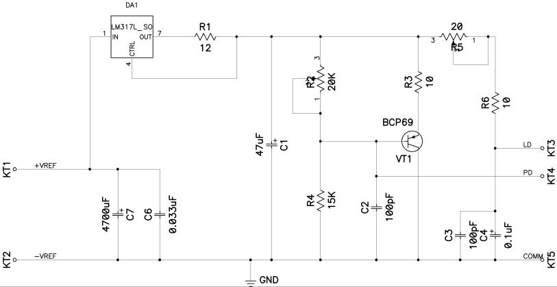
This includes immunity to power line transients as well as those that may occur during power-on and power-off cycling. The parameters of many electronic components like ICs are rarely specified during periods of changing input power. Special laser diode...
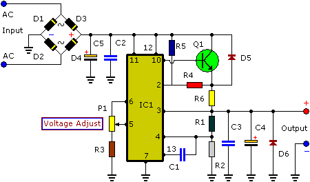
This power supply is designed as either an auxiliary or a permanent power source for various circuits that require a stabilized DC voltage ranging from 3 to 30V, with a maximum current consumption of 3A. Additionally, this power supply...
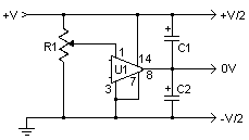
This simple and inexpensive circuit can produce a dual (positive and negative) voltage from a single supply input. It is therefore extremely useful for powering opamp and other circuits that require a dual voltage from a single battery. The...