
Bipolar-reference-source
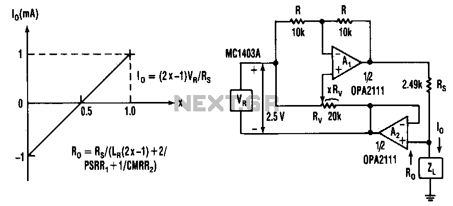
This current source provides continuous control over the magnitude and polarity of its amplifier gain, requiring only a single voltage reference. The circuit comprises a voltage-amplifier circuit (A1) with a gain-setting resistor (Rs) and a bootstrap-follower amplifier (A2). The bootstrapping process transforms the circuit into a current source, enabling the load to be grounded. Any voltage developed across the load (ZL) is fed back to the reference and voltage amplifier, rendering their functions immune to that voltage. Consequently, the current-source circuitry floats rather than the load. The voltage reference is connected to both the inverting and non-inverting inputs of A1, ensuring a balanced combination of positive and negative gain. The inverting connection features equal feedback resistors (R), providing a gain of -1, while the non-inverting connection varies based on the fractional setting (X) of the potentiometer (Rv). This setting controls the non-inverting gain, and adjusting it counteracts some of the effects of the inverting gain. The value of X represents the portion of Rv's resistance from the non-inverting input of A1 to the temporarily grounded output of A2. The current varies with X ±1 mA across the potentiometer's extremes.
This current source circuit is designed to maintain stable performance across varying load conditions. The architecture of the circuit allows for an adaptable gain structure, which is essential in applications where precision control of current is required. The voltage amplifier (A1) plays a crucial role in determining the gain characteristics of the circuit. By utilizing a gain-setting resistor (Rs), the designer can calibrate the circuit to meet specific operational requirements.
The bootstrap-follower amplifier (A2) enhances the circuit's ability to provide a stable output current, even when the load impedance changes. This is particularly advantageous in scenarios where the load may fluctuate, as the bootstrapping technique effectively isolates the load from the current source, thereby maintaining consistent performance.
The feedback mechanism employed in this circuit is vital for ensuring that the amplifier's gain remains unaffected by the load voltage. This is achieved through the careful design of the feedback network, which includes the equal feedback resistors (R) connected to the inverting input of A1. The result is a gain of -1, which is critical for stabilizing the circuit's response.
Furthermore, the non-inverting gain control, facilitated by the potentiometer (Rv), allows for fine-tuning of the output current. The variable setting (X) enables adjustments to be made quickly and efficiently, ensuring that the circuit can adapt to the desired operating conditions. The relationship between the potentiometer setting and the output current is linear, providing an intuitive control mechanism for users.
Overall, this current source design exemplifies a sophisticated approach to amplifier gain control, integrating feedback and bootstrapping techniques to achieve a robust and reliable circuit suitable for various electronic applications.This current source has continuous control of the magnitude and polarity of its amplifier gain and needs only one voltage reference. The circuit includes reference ~, voltage-amplifier circuit A1 with gainsetting resistor Rs, and bootstrap-follower amplifier A2.
The bootstrapping converts the circuit to a current source and allows the load to be grounded. Any voltage developed across load ZL feeds back to the reference and voltage amplifier, making their functions inunune to that voltage. Then the current -source circuitry floats, instead of the load. The voltage reference is connected to both the inverting and noninverting inputs of A1; this provides a balanced combination of positive and negative gain.
The inverting connection has equal feedback resistors, R, for a gain of -1, and the noninverting connection varies according to the fractional setting, X, of potentiometer R v· X controls the noninverting gain and adjusting it counters the effect of some of the inverting gain. The value of X is the portion of Rv"s resistance from the noninverting input of A1 to the temporarily grounded output of A2.
Between potentiometer extremes, the current varies with X ±1 mA. 🔗 External reference