Broadcast-band-rf-amplifier

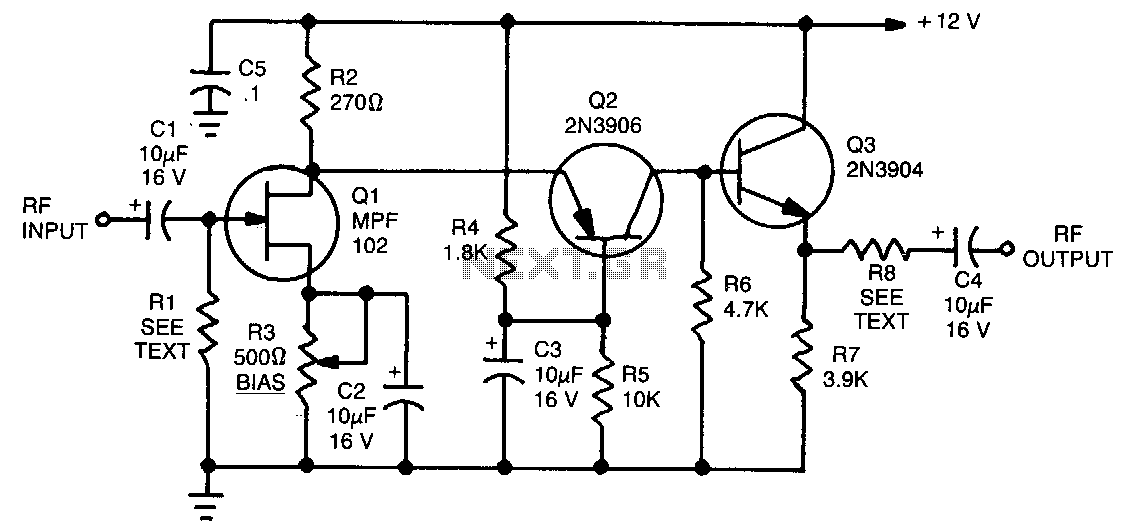
The circuit features a frequency response ranging from 100 Hz to 3 MHz, with a gain of approximately 30 dB. Field-effect transistor Q1 is configured in a common-source self-biased mode. An optional resistor R1 allows for the adjustment of the input impedance to a desired value, typically set at 50 ohms. The signal is then directly coupled to Q2, which operates as a common-base circuit, effectively isolating the input and output stages while providing exceptional stability for the amplifier. Lastly, Q3 functions as an emitter follower to deliver a low output impedance of around 50 ohms. For applications requiring higher output impedance, resistor R8 can be included, which will adjust the impedance based on the formula: RS = RoUT - 50. Alternatively, the output capacitor C4 can be connected directly to the emitter of Q3.
The circuit described operates as a high-frequency amplifier, effectively utilizing field-effect transistors (FETs) for signal processing. The configuration of Q1 in the common-source mode allows for significant voltage gain while maintaining a stable operating point due to its self-biasing feature. The optional resistor R1 provides flexibility in setting the input impedance, which is crucial for matching the amplifier with various signal sources to optimize power transfer and minimize reflections.
The coupling of the output from Q1 to Q2, a common-base configuration, is instrumental in ensuring that the amplifier retains high stability across its frequency response. This stage is particularly effective at handling high-frequency signals, as it offers low input impedance, allowing for efficient signal transfer while isolating the previous and subsequent stages.
Q3, acting as an emitter follower, serves the purpose of buffering the output to maintain low output impedance, which is essential for driving loads effectively without significant signal loss. The inclusion of resistor R8 provides an option to increase output impedance for specific applications, allowing for greater adaptability in circuit design. The formula provided for calculating output impedance indicates a direct relationship between the added resistance and the resulting output impedance, allowing for precise adjustments based on the requirements of the connected load.
The use of output capacitor C4 directly connected to the emitter of Q3 ensures that any DC offset is blocked, allowing only AC signals to pass to the subsequent stage or load. This design consideration is vital for protecting downstream components from potential damage due to DC levels while maintaining signal integrity. Overall, this circuit exemplifies a well-thought-out design that balances gain, stability, and flexibility in a high-frequency application.The circuit has a frequency response ranging from 100Hz to 3 MHz; gain is about 30 dB. Field-effect transistor Q1 is configured in the common-source self-biased mode. Optional resistor R1 allows you to set the input impedance to any desired value; commonly, it will be 50 0. The signal is then direct coupled to Q2, a common-base circuit that isolates the input and output stages and provides the amplifier"s exceptional stability.
Last, Q3 functions as an emitter follower, to provide low output impedance at about 50 O.!fyou need higher output impedance, include resistor R8. It will affect impedance according to this formula: RS "" RoUT -50. Otherwise, connect output capacitor C4 directly to the emitter of Q3.