
Build A Byte Blaster Circuit
The schematic in question is integral to understanding the operation of the Altera ByteBlaster, a device used for programming and debugging FPGA and CPLD devices. The 74LS244 octal buffer plays a crucial role in this circuit, providing signal buffering and isolation between the programming interface and the target device. This is particularly important to maintain signal integrity and protect sensitive components from potential damage due to high current levels.
In this design, the use of current-limiting resistors is essential. These resistors are strategically placed to prevent excessive current flow that could occur during signal transitions, which could otherwise lead to overheating or failure of the 74LS244. The careful selection of these resistors ensures that the circuit operates within safe limits, allowing for reliable performance across varying conditions.
The 10-pin connector is a critical interface for the ByteBlaster, enabling communication between the programming device and the target hardware. Although the connector features 10 pins, only 8 are utilized in the JTAG configuration. This pin arrangement is designed to facilitate straightforward connections while minimizing the risk of miswiring. Each pin's function is labeled clearly, aiding in the assembly and troubleshooting processes.
The updated ByteBlaster MV design provides enhancements over the original model, particularly in power management. By addressing the power limitations of some parallel ports, it ensures that the device can operate effectively across a wider range of systems. This advancement is vital for users who require compatibility with various computer architectures and configurations.
In summary, the schematic derived from the Altera ByteBlaster documentation encapsulates essential design elements, including the role of the 74LS244 buffer, the importance of current-limiting resistors, and the functionality of the 10-pin connector. Understanding these components is crucial for effective implementation and operation of the ByteBlaster in programming and debugging applications.This schematic is taken directly from the Altera ByteBlaster datasheet or manual. They spill out all the fine print and details of how the connector works & what connections go where. Find the datasheet on their website or through google and give it a good read through. The 74LS244 is a Low Power Schottky Octal Buffer. A downside to using this ch ip in this design is that some computer parallel ports may not offer enough power for this circuit. The ByteBlaster MV is an updated design that solves this problem, something we`ll explore later on. These resisitors act as simple current limiting resistors. They make sure no surge of current can come from the JTAG or Parallel ports that might potentially damage the 74LS244. The pins for the 10-Pin connector are again clearly labeled. Notice that only 8 of the 10 pins are actually connected to the JTAG style connector. 🔗 External reference
Related Circuits
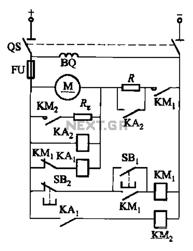
The circuit illustrated in Figure 3-196 features a starting resistance level and an undervoltage relay (KAz) that is controlled by the removal of the startup resistor. It also includes dynamic braking for shutdown purposes. The undervoltage relay (KAL) operates...
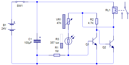
This circuit can provide various utilities, such as an alarm, door opening mechanism, or lighting control for a garden or courtyard, depending on the user's creativity. The operating principle relies on the characteristics of a photoelectric photocell, which alters...
This is a simple frequency counter designed to monitor the 240VAC mains supply. It has a frequency range of 0-999Hz, making it suitable for use with 400Hz equipment as well. Standard TTL/CMOS logic is utilized for the counters and...

RS-232 Serial Interface Status Indicator Circuit. This circuit utilizes a single logic integrated circuit (IC) to indicate the transmission (TXD) and reception (RXD) statuses of a serial interface. The RS-232 Serial Interface Status Indicator Circuit is designed to provide visual...
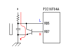
A Darlington connection-type transistor is utilized for driving the coil. In this configuration, two stages of transistors are connected in series, resulting in a high current gain, where the "hfe" of the Darlington transistor is the product of the...
Army Radio Sales Co. specializes in military communications equipment for ham radio operators and collectors. The company offers a variety of military radios from various countries for sale and also engages in the buying and swapping of military radios...