
Capacitor-discharge-high-voltage-generator
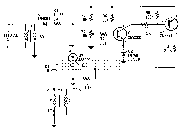
A step-down transformer T1 reduces the incoming line voltage to approximately 48 Vac, which is then rectified by diode D1. The resulting direct current charges capacitor C1 through a current-limiting resistor R1 to a voltage level set by R4. When the voltage at the wiper of R4 reaches about 8.6 V, transistor Q1 begins to turn on, allowing current to flow through R7 and the base-emitter junction of transistor Q2. This action turns on Q2, which provides a positive voltage to the gate of the silicon-controlled rectifier (SCR) Q3. The positive voltage at the gate causes Q3 to conduct, discharging C1 through the primary winding of the step-up transformer T2. This discharge generates a high-voltage arc at output terminal X. The output voltage from T2 is determined by the capacitance of C1, the voltage across C1, and the turns ratio of transformer T2. The frequency or pulse rate of the high voltage is influenced by the resistance of T1's primary and secondary windings, the value of R1, and the capacitance of C1. A lower resistance or capacitance results in a higher output pulse rate, while the peak output voltage remains constant as long as the capacitance of C1 does not change.
The circuit described employs a step-down transformer, T1, which effectively reduces the line voltage to a manageable level suitable for further processing. The rectification of the AC voltage by diode D1 converts the alternating current into direct current, which is essential for charging capacitor C1. The charge level of C1 is controlled by resistor R1, which serves to limit the current and prevent excessive charging that could damage the components.
Transistor Q1 acts as a switch that is triggered when the voltage at the wiper of resistor R4 reaches a predetermined threshold of approximately 8.6 V. This threshold is critical as it ensures that Q1 only activates when sufficient voltage is present, thereby providing a stable operation for the circuit. Once Q1 is activated, it allows current to flow through R7, which then biases transistor Q2 into conduction. The role of Q2 is to amplify the control signal to activate the SCR Q3.
The SCR Q3 is a key component in this circuit, as it allows for the rapid discharge of capacitor C1 through the primary winding of transformer T2. This rapid discharge is what generates the high-voltage pulse at output terminal X. The design of transformer T2, specifically its turns ratio, plays a significant role in determining the output voltage. The relationship between the input voltage across C1 and the turns ratio will dictate the resulting high-voltage output.
The frequency of the high-voltage output is a function of several factors, including the resistances in T1's windings, the value of resistor R1, and the capacitance of C1. By adjusting these components, one can fine-tune the output characteristics to meet specific requirements. It is important to note that while the pulse rate can be increased by lowering the resistance or capacitance, the peak voltage will remain stable as long as the capacitance of C1 is maintained. This mechanism allows for precise control over both the voltage and frequency of the output, making the circuit suitable for various applications requiring high-voltage pulses.Stepdown transformer T1 drops the incoming line voltage to approximately 48 Vac which is rectified by diode D1; the resultant de charges capacitor C1-through current limiting resistor Rl-to a voltage level preset by R4. When the voltage on R4"s wiper reaches about 8.6 V, Q1 begins to turn on, drawing current through R7 and the base-emitter junction of Q2.
Q2 turns on and supplies a positive voltage to the gate of silicon-controlled rectifier Q3. The positive gate voltage causes Q3 to conduct, thereby discharging C1 through the primary winding of step-up transformer T2, which results in a high-voltage arc at output terminal X. The voltage developed at T2"s output is determined by the value of C1, the voltage across C1, and the turns ratio of transformer T2.
The frequency or pulse rate of the high voltage is determined by the resistance of T1 "s primary and secondary windings, the value of R1, and the value of Cl. The lower the value of each item, the higher the output pulse rate; the peak output voltage will only remain unchanged if C1"s value remains unchanged.
🔗 External reference