


Bug Detector Circuit
#bug detector
#op-amp
#transistor
#high-pass filter
#antenna
#amplifier
#security
#RF detection
#signal processing
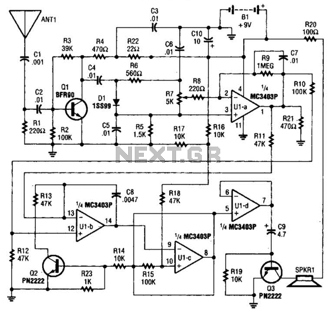
Description: The circuit is constructed around a single integrated circuit (U1), specifically an MC3403P quad op-amp, three transistors (Q1-Q3), and several supporting components. It receives its input from the antenna (ANT1). The signal is processed through a high-pass filter composed of capacitors C1, C2, and resistor R1, which removes unwanted 60-Hz noise from nearby power lines or cords typically found in residential and commercial environments. Following the high-pass filter, the signal is directed to transistor Q1, which provides a 10-dB gain for frequencies ranging from 1 to 2000 MHz, facilitating amplification. Resistors R2, R3, and R4 constitute the biasing network for Q1. The amplified signal is then AC-coupled through capacitor C4 and the wiper of resistor R7, which serves as the sensitivity control, to the inverting input (pin 2) of U1-a. Op-amp U1-a is configured as a very high-gain amplifier.
With no signal input from ANT1, the output at pin 1 of U1-a remains near ground potential. When a signal from the antenna is applied to the base of Q1, it activates, generating a negative-going voltage at the cathode of diode D1. This voltage is then fed into pin 1 of U1-a, which amplifies and inverts the signal, resulting in a positive-going output at pin 1. Op-amps U1-b and U1-c, along with other components including Q2 and resistors R10 through R18, are configured to create a voltage-controlled oscillator (VCO) that operates within the audio frequency range. As the output from U1-a increases, the frequency of the VCO also increases. The output from the VCO, located at pin 8 of U1-c, is then sent to U1-d, which is set up as a non-inverting unity-gain buffer amplifier. The output from U1-d is utilized to drive transistor Q3, which subsequently powers the output speaker.
This circuit effectively amplifies signals received from the antenna while filtering out low-frequency noise, ensuring that only the desired frequency range is processed. The use of a high-pass filter at the input stage is crucial for maintaining signal integrity in environments prone to electrical interference from AC power sources. The configuration of the op-amps allows for significant amplification and signal inversion, which is essential for driving the VCO. The VCO's frequency modulation based on the amplified signal provides versatility in audio applications, enabling the circuit to adapt to varying input conditions. The final stage, comprising the buffer amplifier and output transistor, ensures that the amplified audio signal is delivered effectively to the speaker, producing clear sound output. Overall, this circuit design exemplifies a robust approach to signal processing in radio frequency applications, combining amplification, filtering, and modulation in a compact and efficient manner. The circuit, built around a single integrated circuit (Ul, an MC3403P quad op amp), three transistors (Q1-Q3), and a few support components,.receives its input from the antenna (ANT1). The signal is fed through a high-pass filter, formed by CI, C2, and Rl, which eliminates bothersome 60-Hz pickup from any nearby power lines or line cords located in and around buildings and homes.
From the high-pass filter, the signal is applied to transistor Ql (which provides a 10-dB gain for frequencies in the 1- to 2000-MHz range) for amplification. Resistors R2, R3, and R4 form the biasing network for Ql. The amplified signal is then ac coupled, via capacitor C4 and resistor R7`s (the sensitivity control) wiper, to the inverting input (pin 2) of Ul-a.
Op amp Ul-a is configured as a very high gain amplifier. With no signal input from ANT1, the output of Ul-a at pin 1 is near ground potential. When a signal from the antenna is applied to the base of Ql, it turns on, producing a negative-go-ing voltage at the cathode of Dl. That voltage is applied to pin 1 of Ul-a, which amplifies and inverts the signal, producing a positive-going output at pin 1.
Op amps Ul-b and Ul-c along with 08, RIO through R18, and Q2 are arranged to form a voltage-controlled oscillator (VCO) that operates over the audio-frequency range. As the output of Ul-a increases, the frequency of the VCO increases, The VCO output, at pin 8 of Ul-c, is fed to the input of Ul-d, which is configured as a noninverting, unity-gain (buffer) amplifier.
The output of Ul-d is used to drive Q3, which, in turn, drives the output speaker.
With no signal input from ANT1, the output at pin 1 of U1-a remains near ground potential. When a signal from the antenna is applied to the base of Q1, it activates, generating a negative-going voltage at the cathode of diode D1. This voltage is then fed into pin 1 of U1-a, which amplifies and inverts the signal, resulting in a positive-going output at pin 1. Op-amps U1-b and U1-c, along with other components including Q2 and resistors R10 through R18, are configured to create a voltage-controlled oscillator (VCO) that operates within the audio frequency range. As the output from U1-a increases, the frequency of the VCO also increases. The output from the VCO, located at pin 8 of U1-c, is then sent to U1-d, which is set up as a non-inverting unity-gain buffer amplifier. The output from U1-d is utilized to drive transistor Q3, which subsequently powers the output speaker.
This circuit effectively amplifies signals received from the antenna while filtering out low-frequency noise, ensuring that only the desired frequency range is processed. The use of a high-pass filter at the input stage is crucial for maintaining signal integrity in environments prone to electrical interference from AC power sources. The configuration of the op-amps allows for significant amplification and signal inversion, which is essential for driving the VCO. The VCO's frequency modulation based on the amplified signal provides versatility in audio applications, enabling the circuit to adapt to varying input conditions. The final stage, comprising the buffer amplifier and output transistor, ensures that the amplified audio signal is delivered effectively to the speaker, producing clear sound output. Overall, this circuit design exemplifies a robust approach to signal processing in radio frequency applications, combining amplification, filtering, and modulation in a compact and efficient manner. The circuit, built around a single integrated circuit (Ul, an MC3403P quad op amp), three transistors (Q1-Q3), and a few support components,.receives its input from the antenna (ANT1). The signal is fed through a high-pass filter, formed by CI, C2, and Rl, which eliminates bothersome 60-Hz pickup from any nearby power lines or line cords located in and around buildings and homes.
From the high-pass filter, the signal is applied to transistor Ql (which provides a 10-dB gain for frequencies in the 1- to 2000-MHz range) for amplification. Resistors R2, R3, and R4 form the biasing network for Ql. The amplified signal is then ac coupled, via capacitor C4 and resistor R7`s (the sensitivity control) wiper, to the inverting input (pin 2) of Ul-a.
Op amp Ul-a is configured as a very high gain amplifier. With no signal input from ANT1, the output of Ul-a at pin 1 is near ground potential. When a signal from the antenna is applied to the base of Ql, it turns on, producing a negative-go-ing voltage at the cathode of Dl. That voltage is applied to pin 1 of Ul-a, which amplifies and inverts the signal, producing a positive-going output at pin 1.
Op amps Ul-b and Ul-c along with 08, RIO through R18, and Q2 are arranged to form a voltage-controlled oscillator (VCO) that operates over the audio-frequency range. As the output of Ul-a increases, the frequency of the VCO increases, The VCO output, at pin 8 of Ul-c, is fed to the input of Ul-d, which is configured as a noninverting, unity-gain (buffer) amplifier.
The output of Ul-d is used to drive Q3, which, in turn, drives the output speaker.
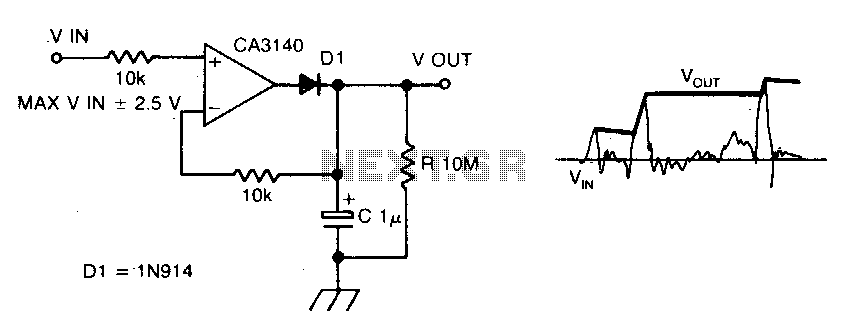
Precision peakvoltage detector
The circuit employs negative feedback exclusively for positive signals. The inverting input receives feedback only when diode D1 is forward biased, which occurs solely with positive input signals. As the positive input signal increases, the output of the operational amplifier...
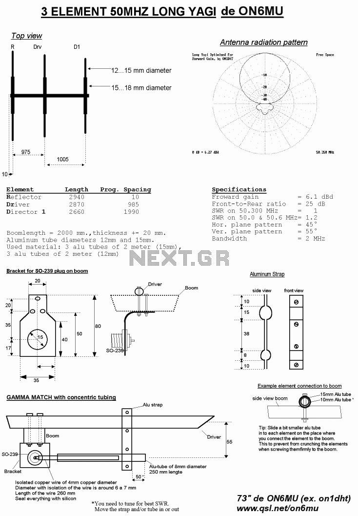
optimized 6 element uhf yagi antenna
The diameter of the antenna elements can range from 5.8 mm, while the dipole diameter can vary from 8 mm to 12 mm, with 12 mm being the recommended size. This adjustment can be made without altering the length or...
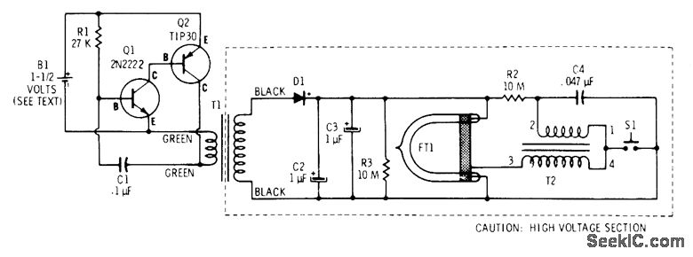
XENON STROBE
A two-transistor oscillator generates pulses at approximately 500 Hz to step up the voltage using a 300-mA filament transformer (T1, Radio Shack 273-1384) for charging storage capacitors C2 and C3, which are 250-V electrolytics. At the same time, capacitor C4...
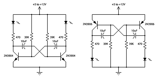
2 Transistor LED Flasher
This is a classic 2-transistor astable multivibrator. Many other NPN small signal or switching transistors can be used, including 2N4401, PN2222, or 2N2222 using the circuit on the left. The circuit can also be inverted using PNP transistors such as...
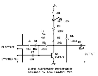
simple microphone preamplifier
The circuit is a simple one-transistor amplifier with an amplification factor of approximately 30-40 dB, which varies depending on the transistor, temperature, and voltage. The dynamic microphone input is a straightforward one-transistor amplifier circuit with no special features. LED D1...
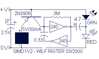
Wilf Rigter`s SIMD1 V2
In the never-ending quest for simplicity, even one extra diode is a price I loathe to pay. To avoid using extra components, it struck me that the two diodes in SIMD1 V1 were connected like the two junctions in one...
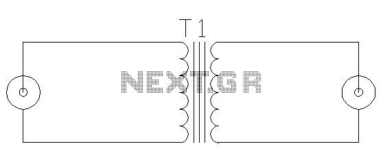
Antenna ground loop Isolator
A ground loop in your AV system caused by antenna connection or TV cable is very common if you have your computer connected to the same system. This type of ground loop problem can be solved by using suitable isolation...
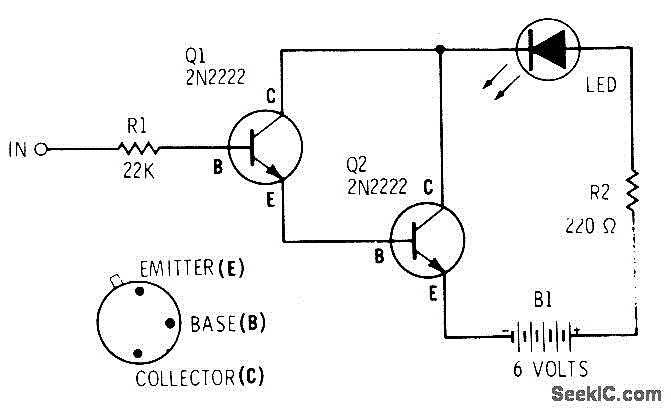
DARLINGTON LOGIC PROBE
A two-transistor Darlington connection offers a very high input impedance, ensuring that it does not load the logic circuit being monitored. This configuration drives an LED that illuminates when a logic high (1) is present at the input.
The two-transistor Darlington...
More op-amp circuits
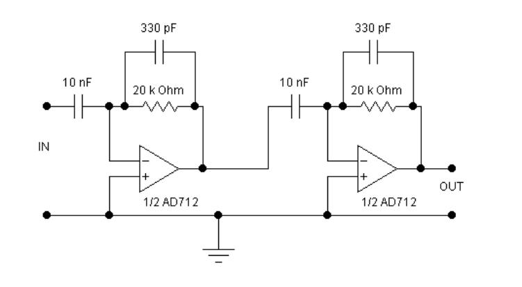
The circuits examined thus far rely on linear feedback for their operation. The magnitude of the signal returned to the negative input is always strictly proportional to the output voltage. Consequently, within the limits defined by the operational amplifier (op-amp),...