


siren alarm circuit diagram usng lm358
#siren
#LM358
#op-amp
#oscillator
#voltage controlled
#alarm
#security
#timer
#switch
#sound generator
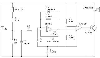
Description: When the switch is pressed, capacitor C3 charges through resistor R4 with a time constant of 0.47 seconds. Upon releasing the switch, C3 discharges more slowly through resistors R7 and R3, with a time constant of approximately 5 seconds. The operational amplifier (op-amp) 358 in this circuit is configured as a voltage-controlled oscillator. When the output of the oscillator (pin 7) goes low, there is still a charge remaining in capacitor C1, which keeps pin 5 below the switching threshold. The current flowing through R7 is proportional to the control voltage on C3. This current discharges C1, causing the voltage at pin 5 to rise towards the switching point at a rate that is proportional to the voltage on C3. Once the switching threshold is reached, pin 7 goes high and initially pulls pin 6 high through C1, causing the op-amp to turn on strongly. However, C3 quickly recharges through diode D2, leading to a decrease in the voltage at pin 5 below the switching threshold, which turns off the op-amp again. The positive pulse output from the op-amp delivers a fixed amount of charge to capacitor C2, slightly increasing the voltage at pin 6. This rise in voltage at pin 6 helps facilitate the rapid turn-off of the op-amp. Additionally, resistors R5 and capacitor C2 introduce a delay in the rise of voltage at pin 6, ensuring a clean output pulse.
The circuit operates effectively as a timing and pulse generation mechanism, utilizing the charging and discharging characteristics of capacitors C3 and C1, along with the feedback and control features of the op-amp 358. The time constants associated with the resistors and capacitors play a critical role in determining the timing behavior of the circuit. The op-amp's configuration allows it to function as a pulse generator, where the interplay between the control voltage on C3 and the discharge characteristics of C1 dictate the timing of the output pulse.
As the switch is engaged, the rapid charging of C3 through R4 initiates the timing cycle. The slow discharge through R7 and R3 creates a delay, allowing for a controlled increase in voltage at pin 5. Once the threshold is reached, the op-amp's output transitions, generating a pulse that is utilized for further circuit functions. The recharging of C3 through D2 is a crucial aspect of the circuit, as it ensures that the op-amp can reset itself quickly after each pulse generation, maintaining the oscillatory behavior.
The use of R5 and C2 is particularly important for shaping the output pulse. By delaying the rise time at pin 6, the circuit can ensure that the output pulse is well-defined and has the necessary duration for downstream applications. This design allows for flexibility in adjusting the timing characteristics by varying the resistor and capacitor values, making it suitable for a range of applications requiring precise timing and control.When the switch is pressed C3 charges up through R4 with a time constant of 0. 47 seconds and when the switch is released C3 begins a slower discharge through R7 and R3 with a time constant of about 5 seconds. The op amp 358 used in this project is set up as a voltage controlled oscillator. When the output of the oscillator (pin 7) switches low the re is a charge remaining in C1 which holds pin 5 below the switching point. Current through R7 is proportional to the control voltage on C3. This current discharges C1 causing the voltage on pin 5 to rise towards the switching point at a rate proportional to the voltage on C3. When the switching point is reached pin 7 switches high and initially pulls pin 6 high via C1. This causes the op amp to temporarily turn on hard. But C3 quickly recharges through D2 causing the voltage on pin 5 to fall below the switching point and causing the op amp to switch off again.
The positive pulse output from the op amp puts a fixed amount of charge into C2 slightly raising the potential of pin 6. This causes the potential on pin 6 to rise and assist the sharp switch off of the op amp. Also R5 & C2 delay the rise on pin 6 long enough to get a good output pulse.
The circuit operates effectively as a timing and pulse generation mechanism, utilizing the charging and discharging characteristics of capacitors C3 and C1, along with the feedback and control features of the op-amp 358. The time constants associated with the resistors and capacitors play a critical role in determining the timing behavior of the circuit. The op-amp's configuration allows it to function as a pulse generator, where the interplay between the control voltage on C3 and the discharge characteristics of C1 dictate the timing of the output pulse.
As the switch is engaged, the rapid charging of C3 through R4 initiates the timing cycle. The slow discharge through R7 and R3 creates a delay, allowing for a controlled increase in voltage at pin 5. Once the threshold is reached, the op-amp's output transitions, generating a pulse that is utilized for further circuit functions. The recharging of C3 through D2 is a crucial aspect of the circuit, as it ensures that the op-amp can reset itself quickly after each pulse generation, maintaining the oscillatory behavior.
The use of R5 and C2 is particularly important for shaping the output pulse. By delaying the rise time at pin 6, the circuit can ensure that the output pulse is well-defined and has the necessary duration for downstream applications. This design allows for flexibility in adjusting the timing characteristics by varying the resistor and capacitor values, making it suitable for a range of applications requiring precise timing and control.When the switch is pressed C3 charges up through R4 with a time constant of 0. 47 seconds and when the switch is released C3 begins a slower discharge through R7 and R3 with a time constant of about 5 seconds. The op amp 358 used in this project is set up as a voltage controlled oscillator. When the output of the oscillator (pin 7) switches low the re is a charge remaining in C1 which holds pin 5 below the switching point. Current through R7 is proportional to the control voltage on C3. This current discharges C1 causing the voltage on pin 5 to rise towards the switching point at a rate proportional to the voltage on C3. When the switching point is reached pin 7 switches high and initially pulls pin 6 high via C1. This causes the op amp to temporarily turn on hard. But C3 quickly recharges through D2 causing the voltage on pin 5 to fall below the switching point and causing the op amp to switch off again.
The positive pulse output from the op amp puts a fixed amount of charge into C2 slightly raising the potential of pin 6. This causes the potential on pin 6 to rise and assist the sharp switch off of the op amp. Also R5 & C2 delay the rise on pin 6 long enough to get a good output pulse.
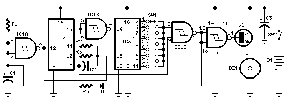
Jogging Timer
This circuit was developed since a number of visitors of this website requested a timer capable of emitting a beep after one, two, three minutes and so on, for jogging purposes. As shown in the Circuit diagram, SW1 is a...

electronic hotel door vulnerability using stealth lock circuit
The term "pentester" refers to a penetration tester, individuals who assess security vulnerabilities. Many high-end hotels globally depend on keycard locks for securing hotel rooms. However, recent incidents of theft have shown that these locks may not be as secure...
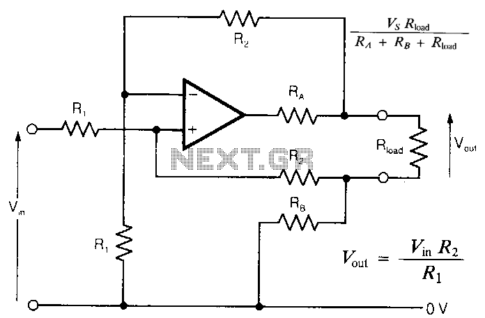
Safe-opamp-circuit
In intrinsically safe applications, it is sometimes necessary to separate sections of circuitry using resistors that limit current under fault conditions. The circuit presented offers an accurate analog output with effectively zero output impedance, despite the presence of resistors in...
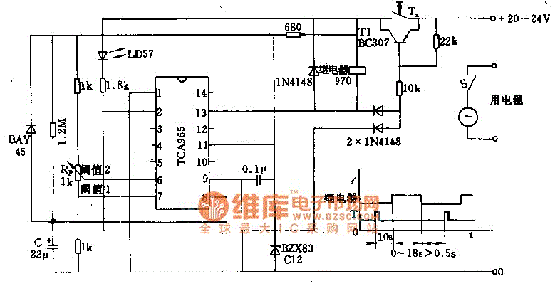
Timer circuit with 106 fixed preset time
The foot 13 between valve value 1 and valve value 2 will draw the transistor base current. If the relay releases, after a recovery time of 0.5 seconds, pressing the key will initiate the switching process again. The timer is...
Timer circuit
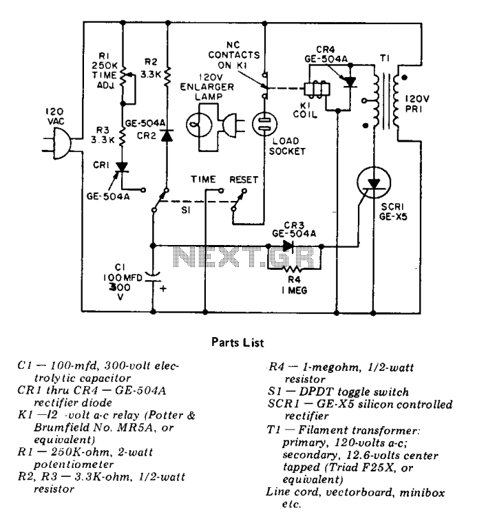
This precision solid-state time delay circuit features both delayed off and delayed on switch functions, which can be interchanged by simply swapping the relay contacts.
The described time delay circuit is designed to provide precise control over the timing of switching...
One-IC two-tones Siren
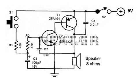
This circuit is designed for children's entertainment and is suitable for installation on bicycles, battery-powered cars, and motorcycles, as well as in models and other games. When switch SW1 is positioned as indicated in the circuit diagram, it reproduces the...
Absolute value amplifier
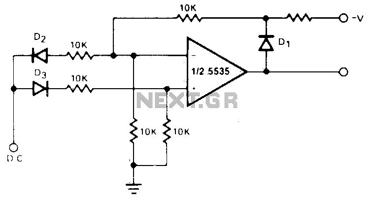
The circuit generates a positive output voltage for either polarity of input. For positive signals, it functions as a non-inverting amplifier, while for negative signals, it operates as an inverting amplifier. The accuracy is poor for input voltages under 1V;...
10 to 1000 MHz Oscillator circuit with RF2506
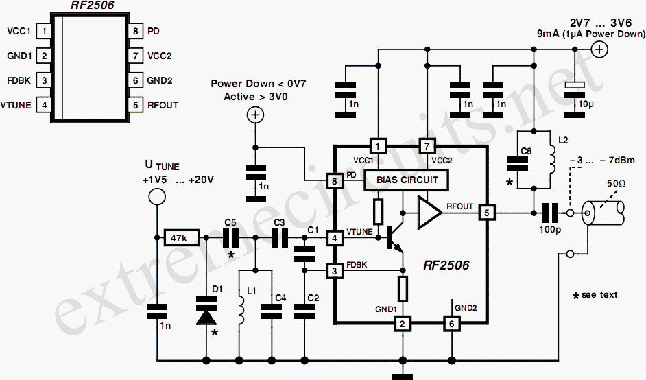
Today, it is no longer necessary to use discrete components for constructing oscillators. Many manufacturers now offer ready-made voltage-controlled oscillator (VCO) integrated circuits (ICs) that require only a few external components to determine the frequency. An example of such an...
One-IC two-tones Sirens
This circuit is designed for children's entertainment and is suitable for installation on bicycles, battery-powered cars, motorcycles, as well as in models and other games. When switch SW1 is positioned as indicated in the circuit diagram, it produces the characteristic...