


A typical circuit for the LM4910 two-channel amplifier
#LM4910
#two-channel amplifier
#audio amplifier
#MSOP
#SO package
#left channel
#right channel
#internal amplifier
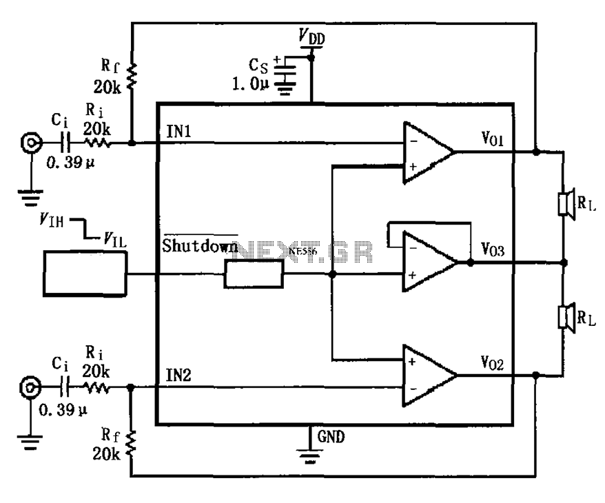
Description: The LM4910 typical circuit is designed for a two-channel amplifier. The left and right channel audio signals are input to the LM4910 (in an MSOP/SO package) at pins 1 and 2. The output signals are delivered from pins 6, 7, and 8, which are connected directly to their respective speakers. The amplifier gain (Av) is determined by the ratio of the feedback resistor (Rf) to the input resistor (Ri). The maximum power consumption is calculated using the formula PDMAX = 4VDD^2 / (2RL). The input of an external resistor and capacitor defines the -3dB bandwidth, with the input capacitor (Ci) calculated as 1/(2 * 20k * 20Hz), which corresponds to approximately 0.39 µF. The LM4910 includes an external control pin (pin 3); when this pin is at a high level (connected to VDD), the amplifier is enabled, while a low level (ground) disables the amplifier.
The LM4910 is a dual-channel audio power amplifier optimized for driving small speakers in portable applications. Its compact size and efficient design make it ideal for battery-powered devices. The left and right audio signals are input through pins 1 and 2, where they are processed by the internal circuitry of the amplifier. The gain of the amplifier is set by external resistors, allowing for flexibility in audio output levels.
The output stage of the LM4910 is capable of delivering significant power to the connected speakers, with the maximum power consumption being a crucial consideration in battery-operated designs. The formula PDMAX = 4VDD^2 / (2RL) indicates that the power output is influenced by the supply voltage (VDD) and the load resistance (RL). This relationship is essential for ensuring that the amplifier operates efficiently without exceeding the power capabilities of the connected speakers.
The -3dB bandwidth is an important parameter that defines the frequency response of the amplifier. By selecting appropriate values for the external resistor and capacitor, designers can tailor the performance of the LM4910 to meet specific audio requirements. The input capacitor value of approximately 0.39 µF, derived from the formula, ensures that the amplifier can handle a wide range of audio frequencies while maintaining sound quality.
Additionally, the LM4910 features a control pin (pin 3) that allows for power management in the circuit. This feature is particularly beneficial in portable applications, as it enables the amplifier to be turned off when not in use, conserving battery life. The ability to control the amplifier's operation through a simple high or low signal enhances the versatility of the LM4910 in various electronic designs. Overall, the LM4910 provides a robust solution for audio amplification in compact electronic devices, combining efficiency with high-quality sound output. As shown for the LM4910 typical circuit for two-channel amplifier. Left and right channel audio signals are input LM4910 (MSOP/SO package) 1,2 feet, after an internal amplifier output pin, respectively, by the 8,7,6, added directly to the respective speakers. Amplifier gain Av -Rf/Ri, the maximum power consumption by the PDMAX 4VDD2/2RL. Input of external resistor and capacitor, respectively determine the input -3dB bandwidth taken Ci 1/(2 20k 20Hz), using about 0.39 F capacitor. LM4910 3 feet off the external control, when 3 feet to VDD (high level) when allowed to work, work prohibited ground (low level).
The LM4910 is a dual-channel audio power amplifier optimized for driving small speakers in portable applications. Its compact size and efficient design make it ideal for battery-powered devices. The left and right audio signals are input through pins 1 and 2, where they are processed by the internal circuitry of the amplifier. The gain of the amplifier is set by external resistors, allowing for flexibility in audio output levels.
The output stage of the LM4910 is capable of delivering significant power to the connected speakers, with the maximum power consumption being a crucial consideration in battery-operated designs. The formula PDMAX = 4VDD^2 / (2RL) indicates that the power output is influenced by the supply voltage (VDD) and the load resistance (RL). This relationship is essential for ensuring that the amplifier operates efficiently without exceeding the power capabilities of the connected speakers.
The -3dB bandwidth is an important parameter that defines the frequency response of the amplifier. By selecting appropriate values for the external resistor and capacitor, designers can tailor the performance of the LM4910 to meet specific audio requirements. The input capacitor value of approximately 0.39 µF, derived from the formula, ensures that the amplifier can handle a wide range of audio frequencies while maintaining sound quality.
Additionally, the LM4910 features a control pin (pin 3) that allows for power management in the circuit. This feature is particularly beneficial in portable applications, as it enables the amplifier to be turned off when not in use, conserving battery life. The ability to control the amplifier's operation through a simple high or low signal enhances the versatility of the LM4910 in various electronic designs. Overall, the LM4910 provides a robust solution for audio amplification in compact electronic devices, combining efficiency with high-quality sound output. As shown for the LM4910 typical circuit for two-channel amplifier. Left and right channel audio signals are input LM4910 (MSOP/SO package) 1,2 feet, after an internal amplifier output pin, respectively, by the 8,7,6, added directly to the respective speakers. Amplifier gain Av -Rf/Ri, the maximum power consumption by the PDMAX 4VDD2/2RL. Input of external resistor and capacitor, respectively determine the input -3dB bandwidth taken Ci 1/(2 20k 20Hz), using about 0.39 F capacitor. LM4910 3 feet off the external control, when 3 feet to VDD (high level) when allowed to work, work prohibited ground (low level).
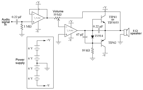
Fundamentals of Electrical Engineering and Class B audio amplifier
It is advisable to obtain TIP41 and TIP42 transistors, which are closely matched NPN and PNP power transistors with dissipation ratings of 65 watts each. If a TIP41 NPN transistor is unavailable, the TIP3055 (available from Radio Shack) serves as...
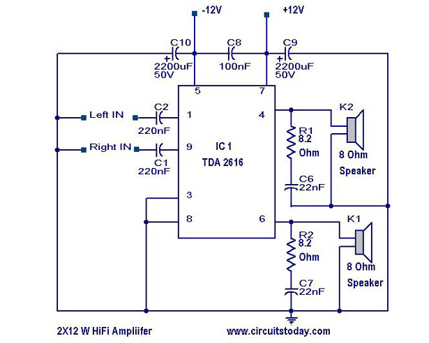
Hi Fi Amplifier circuit
A simple Hi-Fi amplifier circuit diagram with a schematic for creating an audio amplifier design using the TDA 2616 IC. This is a stereo power amplifier suitable for radio, tape, and television applications, delivering 2 x 12 watts, totaling 24...
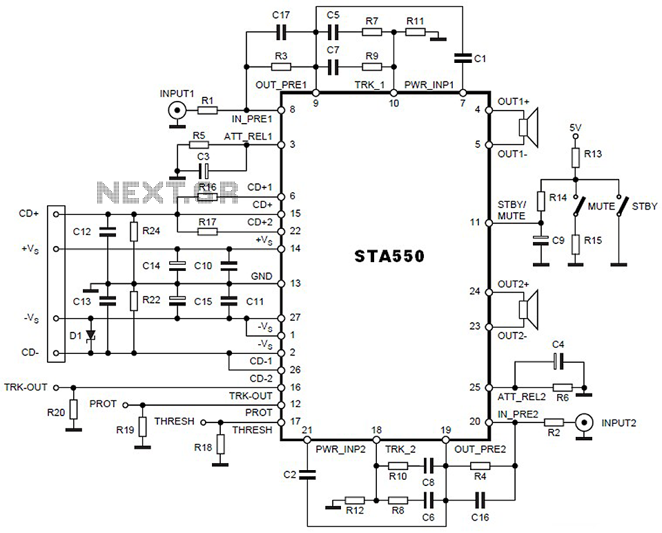
STA550 - 2 x 70W Audio Amplifier Circuit
This is a 2 x 70W audio power amplifier circuit built using a single IC STA550. The amplifier circuit requires a few external components, primarily resistors and capacitors, and is straightforward to design. The STA550 audio amplifier can provide a...
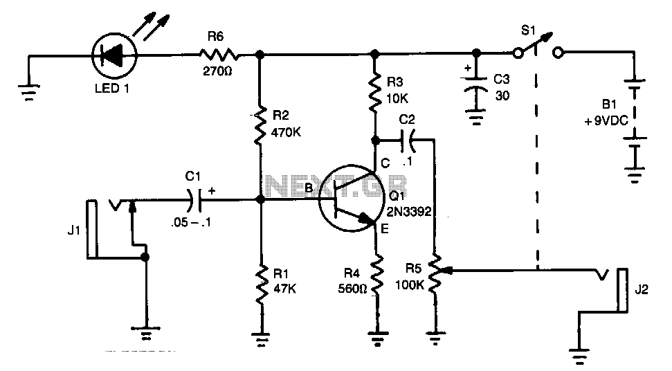
20Db-audio-booster
The amplifier's gain is nominally 20 dB. Its frequency response is primarily influenced by the values of a few components, mainly C1 and R1. The values in the schematic diagram yield a response of ±3.0 dB from approximately 120 Hz...
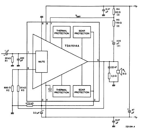
TDA1514 audio amplifier circuit design electronic project
The TDA1514 audio amplifier circuit design is an electronic project capable of delivering high audio power output using a specialized audio integrated circuit (IC) and a few common components. Manufactured by Philips Semiconductor, the TDA1514 audio IC can provide an...
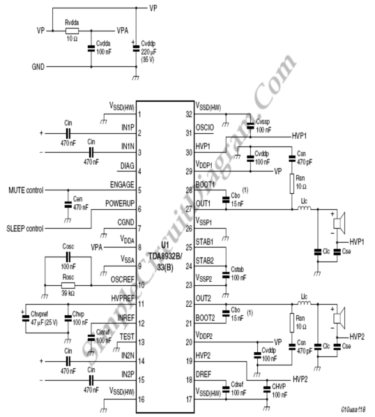
TDA8932B D Audio Amplifier
The following circuit diagram represents a simplified application circuit of the TDA8932B/33(B) device when operated from an asymmetrical (single) supply. To streamline the design for an asymmetrical supply in a single-ended (SE) configuration, the TDA8932B/33(B) incorporates three integrated half-supply voltage...
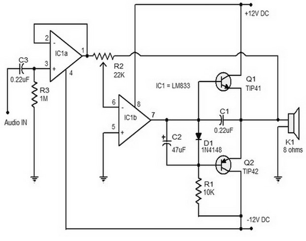
15w class b audio amplifie0r
The 15W Class B audio amplifier circuit presented here is a straightforward Class B audio amplifier utilizing the TL082 operational amplifier, along with TIP41 and TIP42 transistors. The LM833 is a dual amplifier known for its high scanning speed and...
20W-audio-amplifier
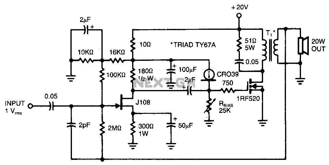
This amplifier provides 20 W of power to an 8-ohm load utilizing a single IRF520 transistor driving a transformer-coupled output stage. The design resembles the audio output stages commonly found in many low-cost radios and phonographs. Distortion remains below 5%...
1.5 12W audio amplifier circuit diagram
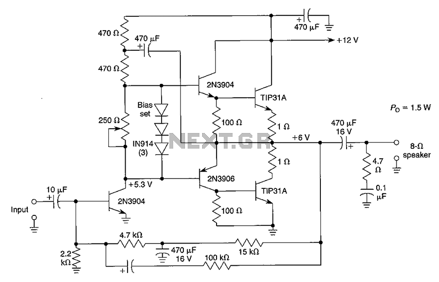
Although the integrated circuit (IC) has largely replaced this circuit, the flexibility of the discrete device design still makes it practical. The components are readily available and cannot easily be eliminated. If desired, a small piece of metal can be...