


OCL power amplifying circuit

Description: Figure 1-30 illustrates an example of an output capacitor-less (OCL) power amplifier circuit, which can be analyzed as follows: In this circuit, transistors VTi and VTz form a single-ended input and a differential input single-ended output amplifier configuration. The signal from the input pole base VTi is amplified by the collector output level of transistor VT3. This configuration consists of a PNP transistor-based emitter amplifier circuit, where PNP transistors are used in conjunction with an NPN transistor to create a midpoint voltage. The arrangement includes transistors VT4, VTs, VT6, and VT7, forming a composite quasi-complementary class AB push-pull output stage. The quiescent bias circuit for the push-pull output stage is designed to allow adjustment of the operating point. The resistor R serves as a negative feedback resistor, which is critical for adjusting the gain of the circuit and stabilizing the midpoint voltage VD. The power supply features two symmetrical voltage sources, V+ and V-, ensuring symmetrical output signals.
In the positive half-cycle of the input signal, the output signal also exhibits a positive half-cycle, during which transistors VT4 and VTs conduct while VT6 and VT7 remain off. If the input signal is sufficiently strong, a positive signal peak can cause VTs to approach saturation, resulting in a voltage drop across the output. If the signal is disregarded, the output voltage during the positive peak is influenced by the load resistance Rl4, with the output voltage reaching a maximum value of V+. Conversely, during the negative peak of the input signal, the output voltage corresponds to a negative peak value. Consequently, the maximum output voltage distortion peaks at 2V. When the input signal is sinusoidal, the maximum power output is determined by the equation Pmax = V+^2 / (2 * RLo). In this scenario, the output power is compared to PE = V+^2 / (r * RLo), allowing for the calculation of circuit efficiency, which is determined to be approximately 78.5%.
This OCL power amplifier circuit is designed to provide high efficiency and low distortion in audio applications. The use of a quasi-complementary output stage allows for improved linearity and reduced crossover distortion, making it suitable for high-fidelity audio amplification. The negative feedback mechanism plays a crucial role in maintaining stability and linear gain across varying load conditions. Additionally, the symmetrical power supply configuration ensures that the amplifier can handle both positive and negative signal excursions effectively, contributing to the overall performance and reliability of the circuit. Proper biasing and component selection are essential for achieving optimal performance, particularly in high-power applications where thermal management and signal integrity are critical.Figure 1-30 is an example of an OCL power amplifier circuit, the following specific analysis: In Figure 1-30, VTi, VTz form a single-ended input and differential input single-e nded output amplifier circuit. Signal from the input pole base VTi, VTi from the mother VT3 collector output level to promote, it is by a PNP transistor consisting of a total of hair emitter amplifier circuit, where the use of the PNP and pre-conjugated to the NPN tube adapter, easy midpoint voltage of dying oVT4, VTs and VT6, VT7 composition of the composite quasi-complementary class AB push-pull power output stage. f) 1, f compliance with the islands push-pull output stage quiescent bias circuit, the output stage in class AB, the island can adjust its operating point adjustment.
R: r is negative feedback resistor for adjusting the gain of the circuit and the static stability midpoint voltage VD. Machine with a V + and V two symmetrical power, the output signal symmetry. Shown in Figure 1-30, in the positive half cycle of the input signal, the output signal is positive half cycle o At this time, VT4, VTs lead pass, VT6, VT7 off.
As long as the input signal is strong enough, you can make when you enter a positive signal peak, VTs approaching saturation and the region, which pressure drop is V mouth. If the signal is ignored Rl4 drop on the output signal of the positive peak voltage v + a 1vais :: : V ~ Similarly, when the input signals negative peak, negative peak output signal voltage is aiming V V ten V a.
Therefore, the circuit output voltage distortion maximum peak value of 2V. If the input signal is sinusoidal crossing, the maximum does not lose the power Ponr-ax y + 2/2RLo In this case, the power source output as compared to PE V + 2/rRLo the two values, in order to calculate the efficiency of the circuit Kun 78.5%.
In the positive half-cycle of the input signal, the output signal also exhibits a positive half-cycle, during which transistors VT4 and VTs conduct while VT6 and VT7 remain off. If the input signal is sufficiently strong, a positive signal peak can cause VTs to approach saturation, resulting in a voltage drop across the output. If the signal is disregarded, the output voltage during the positive peak is influenced by the load resistance Rl4, with the output voltage reaching a maximum value of V+. Conversely, during the negative peak of the input signal, the output voltage corresponds to a negative peak value. Consequently, the maximum output voltage distortion peaks at 2V. When the input signal is sinusoidal, the maximum power output is determined by the equation Pmax = V+^2 / (2 * RLo). In this scenario, the output power is compared to PE = V+^2 / (r * RLo), allowing for the calculation of circuit efficiency, which is determined to be approximately 78.5%.
This OCL power amplifier circuit is designed to provide high efficiency and low distortion in audio applications. The use of a quasi-complementary output stage allows for improved linearity and reduced crossover distortion, making it suitable for high-fidelity audio amplification. The negative feedback mechanism plays a crucial role in maintaining stability and linear gain across varying load conditions. Additionally, the symmetrical power supply configuration ensures that the amplifier can handle both positive and negative signal excursions effectively, contributing to the overall performance and reliability of the circuit. Proper biasing and component selection are essential for achieving optimal performance, particularly in high-power applications where thermal management and signal integrity are critical.Figure 1-30 is an example of an OCL power amplifier circuit, the following specific analysis: In Figure 1-30, VTi, VTz form a single-ended input and differential input single-e nded output amplifier circuit. Signal from the input pole base VTi, VTi from the mother VT3 collector output level to promote, it is by a PNP transistor consisting of a total of hair emitter amplifier circuit, where the use of the PNP and pre-conjugated to the NPN tube adapter, easy midpoint voltage of dying oVT4, VTs and VT6, VT7 composition of the composite quasi-complementary class AB push-pull power output stage. f) 1, f compliance with the islands push-pull output stage quiescent bias circuit, the output stage in class AB, the island can adjust its operating point adjustment.
R: r is negative feedback resistor for adjusting the gain of the circuit and the static stability midpoint voltage VD. Machine with a V + and V two symmetrical power, the output signal symmetry. Shown in Figure 1-30, in the positive half cycle of the input signal, the output signal is positive half cycle o At this time, VT4, VTs lead pass, VT6, VT7 off.
As long as the input signal is strong enough, you can make when you enter a positive signal peak, VTs approaching saturation and the region, which pressure drop is V mouth. If the signal is ignored Rl4 drop on the output signal of the positive peak voltage v + a 1vais :: : V ~ Similarly, when the input signals negative peak, negative peak output signal voltage is aiming V V ten V a.
Therefore, the circuit output voltage distortion maximum peak value of 2V. If the input signal is sinusoidal crossing, the maximum does not lose the power Ponr-ax y + 2/2RLo In this case, the power source output as compared to PE V + 2/rRLo the two values, in order to calculate the efficiency of the circuit Kun 78.5%.
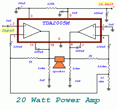
20 watt power amplifier
This integrated circuit (IC) chip is specifically designed for power boosting applications in automobiles. It features self-protection mechanisms against short circuits and thermal issues. In the bridge configuration depicted, it can deliver 20 watts of power to a 2-ohm speaker...
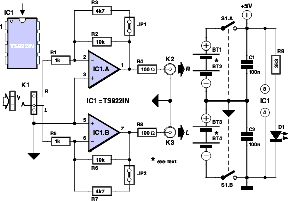
Power Amplifier 6
This simple circuit is designed to provide an output power of approximately 1 watt when connected to a 9-volt power supply. The key advantage of this circuit is its use of a dual Darlington configuration, which increases the input impedance...
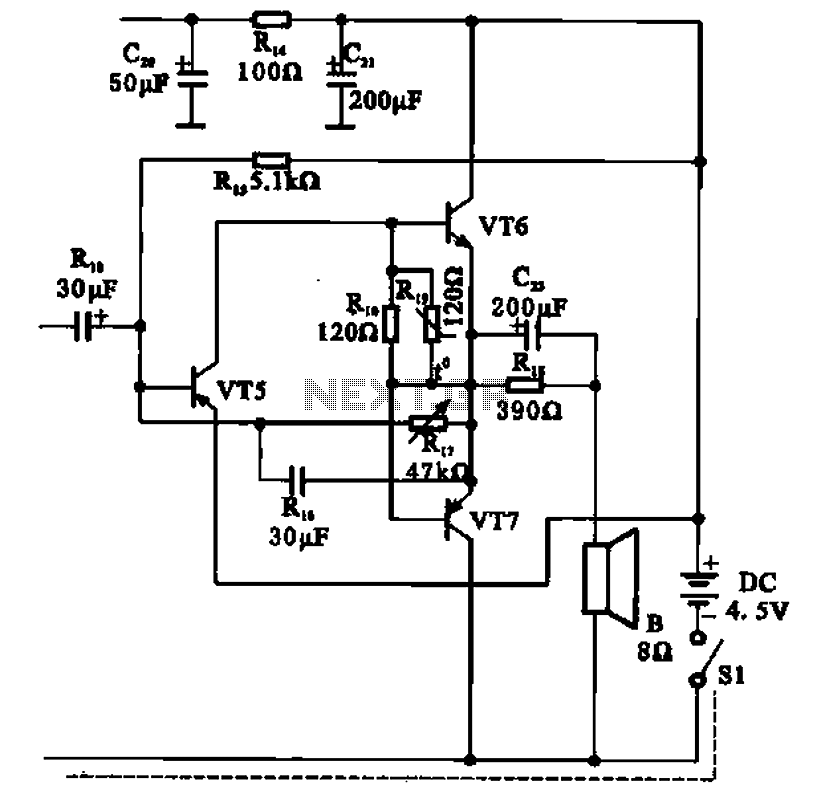
OTL transistor radio in a power amplifier circuit
The transistor radio features a common output transformerless (OTL) power amplifier circuit. The VT5 component serves as the bias resistor for the driver stage. VT6 and VT7 form a complementary symmetry configuration, with VT6 being a germanium NPN transistor and...
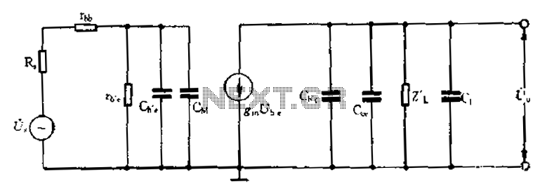
Common emitter amplifier circuit resistance and capacitance coupled basic
Common emitter amplifier circuit with resistance and capacitance coupling.
The common emitter amplifier circuit is a fundamental configuration in analog electronics, widely utilized for its ability to amplify voltage signals. This circuit employs a bipolar junction transistor (BJT) as the active...
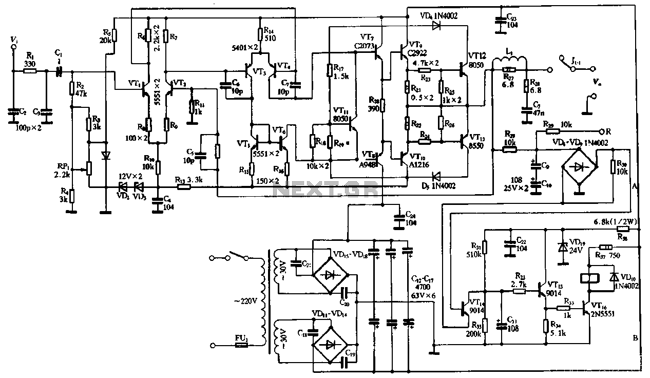
2SC2922 and 2SA1216 or 2SC3264 and 2SA1295 power amplifier circuit
The performance of the amplifiers 2SC2922 and 2SA1216 (or 2SC3264 and 2SA1295) is excellent, featuring good linearity and strong overload capabilities. These devices are utilized as high-fidelity power amplifier stages, demonstrating outstanding performance. The circuit, as illustrated in Figure 2-30,...
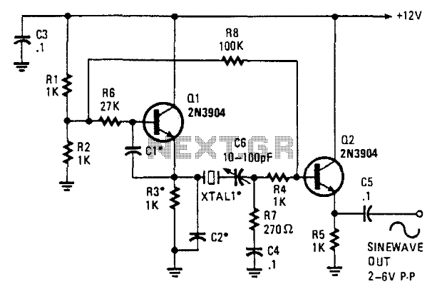
Two-Transistor Sine-Wave Oscillator
This oscillator employs two transistors and operates the crystal in its fundamental mode. Capacitors CT and C2 should be approximately 2,700 pF for 1 MHz, 680 pF for 5 MHz, and 330 pF for 10 MHz. A capacitance of 150...
Complete Solid state M-9 Power Amplifier
The following circuit illustrates a complete solid-state M-9 power amplifier circuit diagram. Features include a DC servo that acts as a loudspeaker protection circuit.
The solid-state M-9 power amplifier circuit is designed to deliver high-quality audio amplification while ensuring the safety...
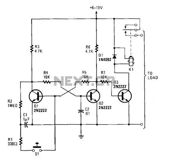
Push-on-push-off electronic switch
Transistors Q1 and Q2 form a flip-flop configuration, while Q3 operates a reed relay. Upon initial power application to the circuit, Q1 and Q3 are in a conducting state, whereas Q2 remains off. A momentary closure of switch S1 triggers...
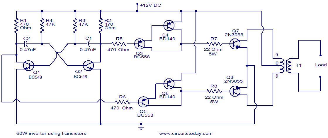
60W inverter using transistors
This circuit diagram illustrates a fully transistorized inverter capable of driving loads of up to 60W. Transistors Q1 and Q2 create a 50Hz astable multivibrator. The output from the collector of Q2 connects to the input of a Darlington pair...