


STK4040x1 made HI-FI amplifier circuit
#STK4040x1
#HI-FI
#audio amplifier
#power amplifier
#sound system
#stereo
#high fidelity
#audio circuit
#amplification
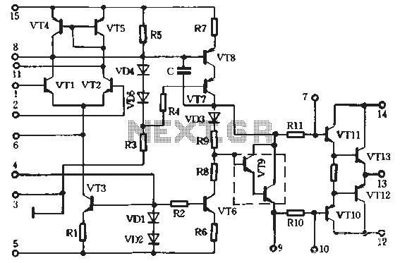
Description: A preferred STK4040xl Fi amplifier circuit exhibits excellent electrical parameters: under specific conditions, the output voltage (Uc) is 43V with a load resistance (RL) of 8 ohms. The circuit is designed to deliver a rated output power of at least 70W, with a maximum harmonic distortion of only 0.008% and a typical value of 0.003%. The frequency response ranges from 20Hz to 20kHz. This amplifier circuit demonstrates outstanding performance, which is relatively rare. The internal equivalent circuit is illustrated in Figure 3-46, highlighting port VT3. The constant current source circuit is composed of resistors R1 and diodes VD1 and VD2, forming a differential pair with transistors VT1 and VT2. This configuration enhances the amplification and common-mode rejection ratio at the input stage. The differential stage outputs a single-ended signal through the base of VT8, which serves as the input for the driver stage formed by VT7 and VT8 in a cascode arrangement. VT7 is connected in a common base configuration, providing significant voltage gain. The grounded base of VT7 offers isolation and shielding, preventing the output signal from feeding back into the input, thereby ensuring stability in the driver stage. To further minimize distortion, VT6 and the current source circuit consisting of R2, VD1, and VD2 serve as the AC load for the driver stage, which is compatible with higher impedance loads (e.g., STK46, STK4151, and other integrated amplifiers), resulting in increased gain and stable operation. The combination of VT9, resistors R8 and R9, and diode VD3 forms a "constant voltage multiplier circuit." The constant values of R8 and R9 are determined by their ratio, which offers lower dynamic resistance compared to conventional series regulator diode circuits, thus enhancing the DC bias stability of the output stage, producing a more symmetrical waveform excitation signal and reducing distortion. The output stage comprises transistors VT10, VT11, VT12, and VT13 configured as symmetrical PNP and NPN Darlington pairs, resulting in a more concise output stage circuit with improved symmetry, linearity, and low distortion characteristics.
The STK4040xl Fi amplifier circuit is characterized by its robust design that integrates various advanced techniques to achieve high performance. The constant current source configuration plays a critical role in maintaining stable biasing conditions across the differential pair, which is pivotal for linear amplification. The use of a cascode arrangement enhances the voltage gain while effectively isolating the output from the input, thereby minimizing feedback that could lead to instability or distortion.
The output stage's design, utilizing Darlington pairs, allows for high current gain while maintaining a compact circuit layout. This configuration not only simplifies the design but also enhances thermal stability and reduces the likelihood of thermal runaway, which is a common concern in high-power amplifier designs. The inclusion of a constant voltage multiplier circuit further stabilizes the output stage's performance, ensuring that the amplifier can handle dynamic loads without significant variations in output voltage or distortion levels.
Overall, the STK4040xl Fi amplifier circuit represents a sophisticated and effective solution for high-fidelity audio amplification, offering exceptional performance metrics that make it suitable for demanding audio applications. The combination of low distortion, wide frequency response, and stable operation under varying loads positions this amplifier as a reliable choice for both professional and consumer audio systems.A preferred STK4040xl Fi amplifier circuit that has good pull electrical parameters: in sv, RL Uc = 43 - 8fl conditions, the rated output power of not less than 70W, the maximum harmonic distortion of only 0.008%, typically 0.003%, 3dB frequency response of 20Hz ~ 20kHz. Such outstanding performance, the amplifier circuit is indeed rare. As shown in Figure 3-46 for its internal equivalent circuit port VT3, the constant current source circuit R 1, VDl.VD2 composition as a differential pair VTl, VTZ common-emitter impedance of the input stage to improve magnification and common-mode rejection ratio .
Differential stage single-ended output signal through VT8 base, as an incentive level input o VT7, VT8 together form an approximate cascode circuit, at the same time, VT7 approximate common base connection, itself a large voltage gain, and VT8 incorporated in and constitute a voltage gain of the driver stage is still high. More importantly, because of the grounded base VT7 with isolation and shielding effect, the output signal VT8 not easily back to the input, to ensure that the driver stage T for more stable.
Into further reduce distortion o VT6 and R2, VD1, VD2 composition of the other current source circuit as a driver stage of AC load, it is more than the S & P resistance Load (eg STK46: 5'STK4151 and many other integrated amplifier), a higher exchange impedance, gain more, work is very stable and reliable 6 VT9. R8R9 and VD3 composition of a "constant voltage multiplier circuit," constant value R8 and R9 mainly by the ratio of the decision.
Compared with the official regulator diode series circuit better, dynamic resistance is smaller, the more the output stage of the DC bias stability, more symmetrical waveform excitation signal, less distortion. VT10.VT11 and VT12.VT13 composition full symmetry PN P NPN Darlington on the tube, so that the output stage circuit more concise, symmetry, good linearity, low distortion.
The STK4040xl Fi amplifier circuit is characterized by its robust design that integrates various advanced techniques to achieve high performance. The constant current source configuration plays a critical role in maintaining stable biasing conditions across the differential pair, which is pivotal for linear amplification. The use of a cascode arrangement enhances the voltage gain while effectively isolating the output from the input, thereby minimizing feedback that could lead to instability or distortion.
The output stage's design, utilizing Darlington pairs, allows for high current gain while maintaining a compact circuit layout. This configuration not only simplifies the design but also enhances thermal stability and reduces the likelihood of thermal runaway, which is a common concern in high-power amplifier designs. The inclusion of a constant voltage multiplier circuit further stabilizes the output stage's performance, ensuring that the amplifier can handle dynamic loads without significant variations in output voltage or distortion levels.
Overall, the STK4040xl Fi amplifier circuit represents a sophisticated and effective solution for high-fidelity audio amplification, offering exceptional performance metrics that make it suitable for demanding audio applications. The combination of low distortion, wide frequency response, and stable operation under varying loads positions this amplifier as a reliable choice for both professional and consumer audio systems.A preferred STK4040xl Fi amplifier circuit that has good pull electrical parameters: in sv, RL Uc = 43 - 8fl conditions, the rated output power of not less than 70W, the maximum harmonic distortion of only 0.008%, typically 0.003%, 3dB frequency response of 20Hz ~ 20kHz. Such outstanding performance, the amplifier circuit is indeed rare. As shown in Figure 3-46 for its internal equivalent circuit port VT3, the constant current source circuit R 1, VDl.VD2 composition as a differential pair VTl, VTZ common-emitter impedance of the input stage to improve magnification and common-mode rejection ratio .
Differential stage single-ended output signal through VT8 base, as an incentive level input o VT7, VT8 together form an approximate cascode circuit, at the same time, VT7 approximate common base connection, itself a large voltage gain, and VT8 incorporated in and constitute a voltage gain of the driver stage is still high. More importantly, because of the grounded base VT7 with isolation and shielding effect, the output signal VT8 not easily back to the input, to ensure that the driver stage T for more stable.
Into further reduce distortion o VT6 and R2, VD1, VD2 composition of the other current source circuit as a driver stage of AC load, it is more than the S & P resistance Load (eg STK46: 5'STK4151 and many other integrated amplifier), a higher exchange impedance, gain more, work is very stable and reliable 6 VT9. R8R9 and VD3 composition of a "constant voltage multiplier circuit," constant value R8 and R9 mainly by the ratio of the decision.
Compared with the official regulator diode series circuit better, dynamic resistance is smaller, the more the output stage of the DC bias stability, more symmetrical waveform excitation signal, less distortion. VT10.VT11 and VT12.VT13 composition full symmetry PN P NPN Darlington on the tube, so that the output stage circuit more concise, symmetry, good linearity, low distortion.
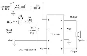
1W Mono Amplifier with TDA7052 circuit diagram
This is an audio amplifier circuit that uses the TDA7052 as the main component, along with five additional components to support its operation. The ideal supply voltage for this circuit is approximately 6-12V, and it does not require a heatsink.
The...
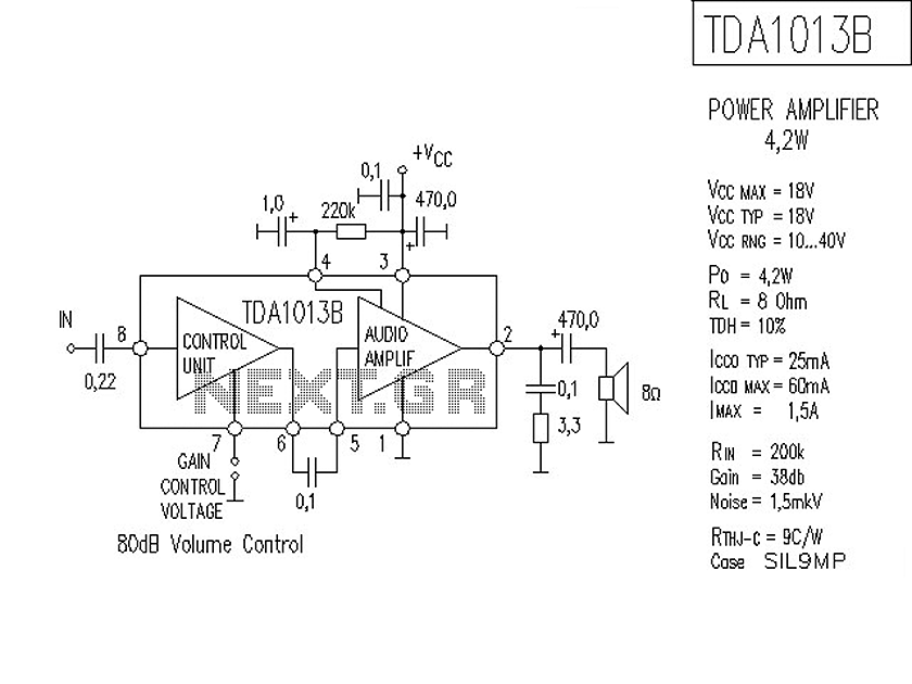
TDA1013B - 4W Audio Amplifier Circuit
The following is a circuit for a 4-watt audio amplifier. The amplifier utilizes an integrated audio amplifier chip, TDA1013B, which is capable of delivering an audio power output of up to 4W at an 8-ohm load. Its wide supply voltage...
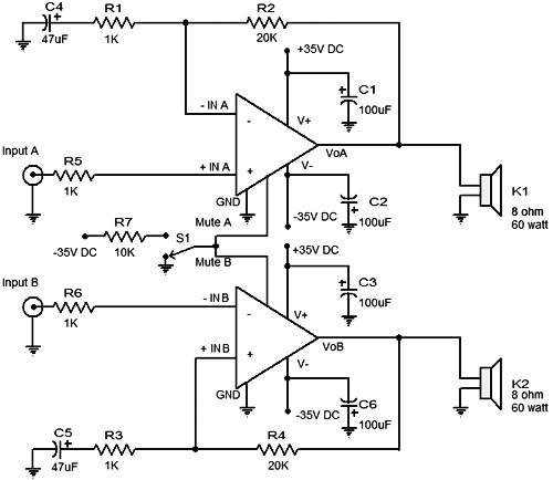
2x60 Watt Stereo Audio Amplifier LM4780
What is so special? First of all, it has a very low harmonic distortion. Typically, manufacturers indicate the maximum power of their products with a harmonic content of 10%. In contrast, this chip achieves a harmonic distortion of only 0.5%...
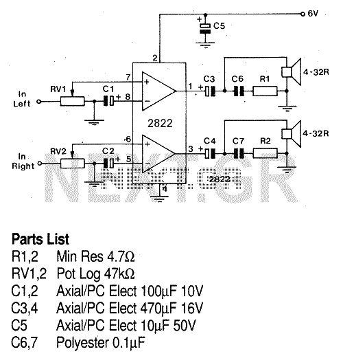
1W stereo Headphone Amp (TDA2822)
A stereo power amp designed for use in portable players and radios. A 3V supply can be used to drive headphones providing 20mW in 32 Ohms per channel. A 9V supply will provide 1W in 8 Ohm per channel for...
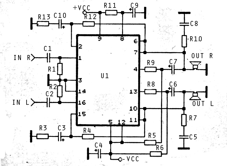
2x30watt home amplifier circuit
The audio amplifier circuit is highly suitable for home use, particularly with subwoofer or woofer speakers. Commonly referred to as a home amplifier, these audio amplifiers are based on integrated circuits (ICs), specifically the STK series, which includes models such...
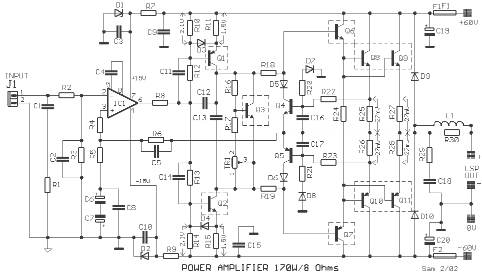
170 Watt audio amplifier
In the drawing, a simple but powerful power amplifier is presented. Its difference from classic designs, which use differential amplifiers in their input, is that this amplifier uses a complete NE5534 at its input. Thus, it is necessary to reduce...
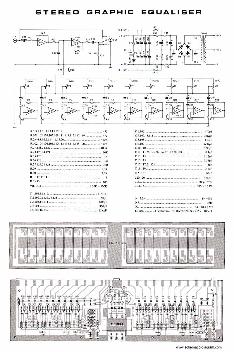
2G—10 Band Stereo Graphic Equaliser circuit diagram
This circuit should be connected prior to the amplifier circuit. To achieve optimal performance, it is recommended to utilize high-quality electronic components such as metal film resistors, MKM capacitors (non-polar), and tantalum capacitors (bipolar). The power supply module can be...
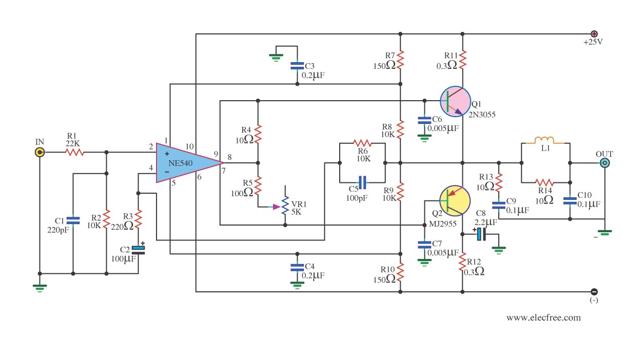
Small class b audio amplifier circuit diagram
When the power supply reaches the circuit and the input signal is applied, the sound signal is processed through capacitor C1 and resistor R1 for signal coupling and noise reduction. The modified signal then reaches pin 3 (non-inverting) of operational...
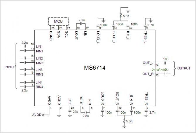
MS6714 4 Stereo Inputs And 1 Stereo Output Volume Tone Balance Loudness And Selectable Input Gain
The MSK4204RH is a radiation-hardened complete H-Bridge microcircuit designed for use in DC brushed motor control applications or Class D switch-mode amplification in space or other harsh operating environments. The internal components have been selected to withstand a total dose...