


Automatic Muting Circuit For Audio Systems PCB
#muting circuit
#LB1403
#pre-amplifier
#BC548
#LA3160
#LA3161
#HA1032
#variable resistor
#comparator
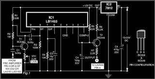
Description: This is a circuit diagram for automatic muting in audio systems utilizing the IC LB1403. The output from a pre-amplifier, such as the LA3160, LA3161, or HA1032, is connected to the base of the amplifier transistor BC548 (T1). A variable resistor VR1 is incorporated to adjust the gain of the input signal. The output from comparator 2 at pin 2 of the LB1403 generates a muting signal at the emitter (point A) of transistor T2, which can be directly linked to the muting pin 4 of an amplifier using the IC LA4440. When the audio input to the circuit is below a specified threshold (approximately 150 mV peak to peak), the output at point A remains high. However, if the input exceeds this threshold, the output drops to around 0V. The capacitor C4 influences the muting delay; a higher capacitance results in a longer muting delay. Modifications to the circuit may be necessary for compatibility with STK series amplifiers, such as STK 4141, 4142, 4152, and 4191, which require a negative polarity voltage for muting. An additional circuit to connect at point A is illustrated in Fig. 2.
The automatic muting circuit described is designed to enhance audio systems by preventing unwanted noise during silent periods. The core component, the LB1403, acts as a comparator that monitors the audio signal level. When the audio signal from the pre-amplifier drops below the defined threshold, the circuit ensures that the output remains active, allowing the audio to pass through without interruption. The variable resistor VR1 allows for fine-tuning of the input signal gain, which is crucial for achieving optimal performance across various audio sources.
Transistor T1, a BC548, operates as a switching device that responds to the input signal from the pre-amplifier. The output from the LB1403's comparator is used to control transistor T2, which serves as the muting switch. When the audio input exceeds the threshold, T2 is activated, resulting in the muting of the audio signal by pulling the output at point A close to 0V. This effectively silences the audio output, preventing any unwanted noise from being transmitted to the amplifier.
Capacitor C4 plays a significant role in determining the muting delay period. By adjusting its capacitance, the designer can control how quickly the muting action occurs when the audio signal falls below the threshold. This delay can help to avoid abrupt audio cut-offs, providing a smoother listening experience.
For compatibility with STK series amplifiers, additional circuitry may be required to adapt the muting function to the specific needs of these devices, particularly regarding the negative voltage requirement for muting. The modifications ensure that the circuit functions correctly within the operational parameters of the STK amplifiers, maintaining the integrity of the audio signal while providing the necessary muting capabilities.Here`s a circuit diagram of automatic muting for audio systems using IC LB1403. The signal from pre-amplifier such as LA3160, LA3161 or HA1032 is connected to the base of the amplifier transistor BC548 (T1). Variable resistor VR1 is used to control the gain of input signal. Comparator 2 output at pin 2 of LB1403 is used for generation of muting s ignal at the emitter (point A) of transistor T2, which can be directly connected to muting pin 4 of amplifier employing IC LA4440. As long as the audio input to the circuit of Fig. 1 is below a certain level (say, 150 mV peak to peak), the output at point A will be high. Once the input crosses this threshold level, the output will be around 0V. Capacitor C4 determines the on`/off` muting delay. Higher the value of this capacitor, greater will be the muting delay period. Slight circuit modification will be needed if this circuit is used with STK series amplifiers, such as STK 4141, 4142, 4152, and 4191, because they need negative polarity voltage for muting.
The additional circuit to be connected at point A in that case is shown in Fig. 2.
The automatic muting circuit described is designed to enhance audio systems by preventing unwanted noise during silent periods. The core component, the LB1403, acts as a comparator that monitors the audio signal level. When the audio signal from the pre-amplifier drops below the defined threshold, the circuit ensures that the output remains active, allowing the audio to pass through without interruption. The variable resistor VR1 allows for fine-tuning of the input signal gain, which is crucial for achieving optimal performance across various audio sources.
Transistor T1, a BC548, operates as a switching device that responds to the input signal from the pre-amplifier. The output from the LB1403's comparator is used to control transistor T2, which serves as the muting switch. When the audio input exceeds the threshold, T2 is activated, resulting in the muting of the audio signal by pulling the output at point A close to 0V. This effectively silences the audio output, preventing any unwanted noise from being transmitted to the amplifier.
Capacitor C4 plays a significant role in determining the muting delay period. By adjusting its capacitance, the designer can control how quickly the muting action occurs when the audio signal falls below the threshold. This delay can help to avoid abrupt audio cut-offs, providing a smoother listening experience.
For compatibility with STK series amplifiers, additional circuitry may be required to adapt the muting function to the specific needs of these devices, particularly regarding the negative voltage requirement for muting. The modifications ensure that the circuit functions correctly within the operational parameters of the STK amplifiers, maintaining the integrity of the audio signal while providing the necessary muting capabilities.Here`s a circuit diagram of automatic muting for audio systems using IC LB1403. The signal from pre-amplifier such as LA3160, LA3161 or HA1032 is connected to the base of the amplifier transistor BC548 (T1). Variable resistor VR1 is used to control the gain of input signal. Comparator 2 output at pin 2 of LB1403 is used for generation of muting s ignal at the emitter (point A) of transistor T2, which can be directly connected to muting pin 4 of amplifier employing IC LA4440. As long as the audio input to the circuit of Fig. 1 is below a certain level (say, 150 mV peak to peak), the output at point A will be high. Once the input crosses this threshold level, the output will be around 0V. Capacitor C4 determines the on`/off` muting delay. Higher the value of this capacitor, greater will be the muting delay period. Slight circuit modification will be needed if this circuit is used with STK series amplifiers, such as STK 4141, 4142, 4152, and 4191, because they need negative polarity voltage for muting.
The additional circuit to be connected at point A in that case is shown in Fig. 2.

Null-detector
In this indicating comparator circuit, R2 sets the hysteresis. If the 741 saturates at ±12 V, the current in R1 will be approximately ±10 mA if a 0.1 V hysteresis is desired. More: Then 0.1 V/10 mA ~ 100.
The indicating...
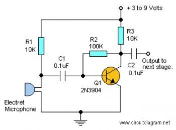
Simple Audio Pre-Amplifier
This straightforward circuit offers substantial amplification for weak audio signals, such as those from an electret microphone. It can be utilized in conjunction with an RF oscillator to create a highly sensitive RF transmitter. The audio microphone preamplifier circuit is...
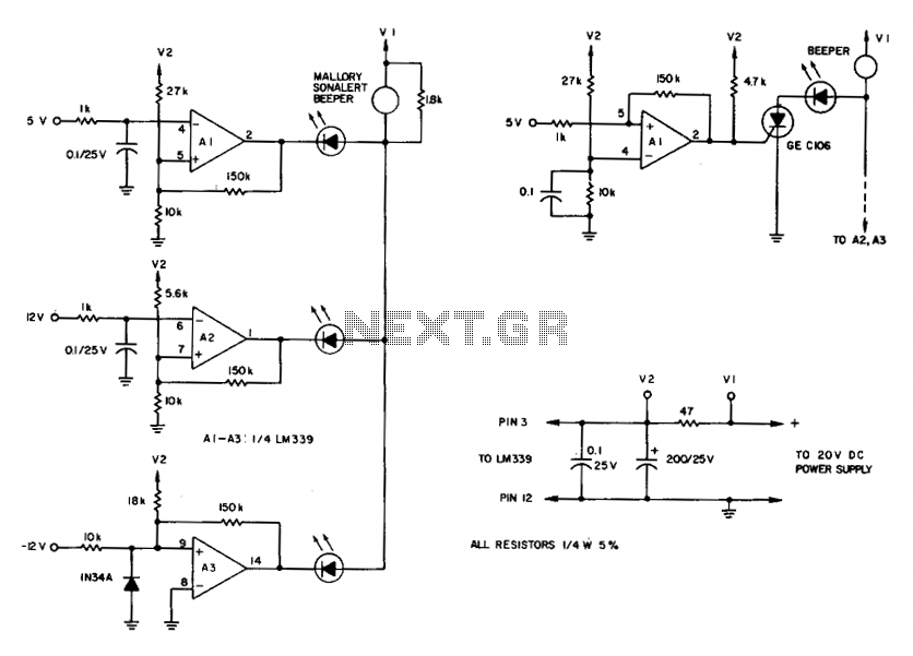
Comparator for over-voltages
To maintain an alarm condition when an overvoltage transient disappears, an SCR should be added to the comparator circuits. For SCR operation, the voltages to the comparator inputs are inverted. The triple-voltage monitoring circuit detects transient power-supply over-voltages. If excessive...
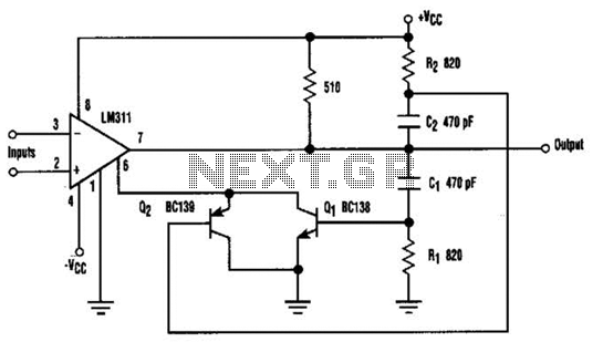
Suppress Jitter With Hysteresis Circuit
When the comparator's output transitions from low to high, the rising edge of the output pulse, differentiated by the Cl/Rl chain, activates Ql. This action blocks the comparator via its strobing input and maintains its output state for a duration...
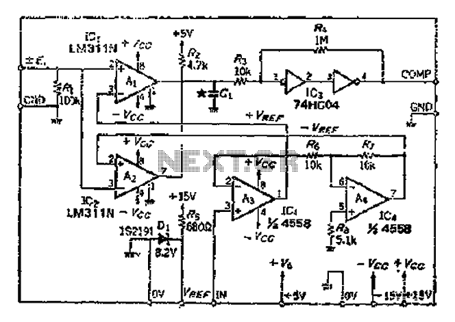
The reference voltage of the symmetrical bipolar comparator
An AI comparator input is connected to a reference resistor (Rl). When the output reaches a specified level, known as VREP (absolute value), the output also stabilizes at this level. The outputs Ai and As are connected to an OR...
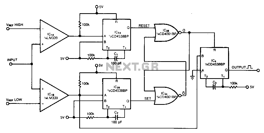
Window-comparator
This window comparator generates an output pulse for each event that occurs within a specified window. Each output pulse signifies an input voltage pulse or level change that exceeds VREFLOW but not VREFHIGH. The monostable multivibrators, IC2A and IC2B, produce...
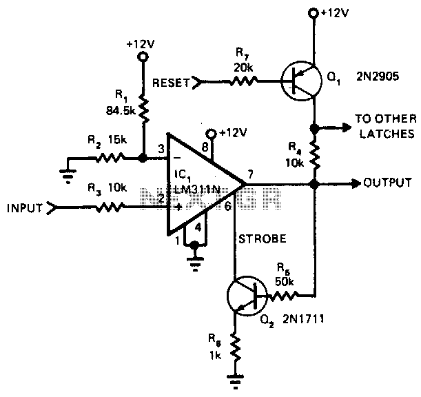
Comparator-latch
The main advantage of this circuit, in comparison to other comparators, is its capability to latch once the input surpasses a specified threshold level. When the input goes beyond this threshold, the output of the LM311N rises. This change activates...
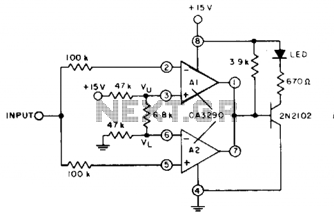
High input comparator
The circuit utilizes both halves of the CA3290 BiMOS dual voltage comparator. The LED will be activated whenever the input signal is above the lower limit (VL) but below the upper limit (Vy).
The circuit design employs the CA3290 BiMOS dual...
Dual limit comparator
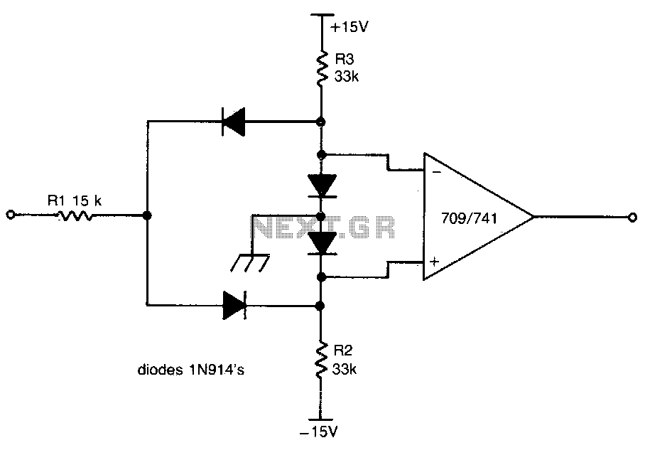
This circuit provides a positive output when the input voltage exceeds 8 volts. Within these limits, the output remains negative. The threshold for the positive output is set by the ratio of resistors R1 and R2, while the threshold for...