


PT2399 | Digital Echo Audio-Circuits
#PT2399
#digital echo
#audio processing
#ADC
#DAC
#CMOS
#echo effect
#sound processing
#audio circuit
#digital delay
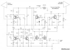
Description: The PT2399 digital echo circuit schematic is an electronic design that utilizes the PT2399 integrated circuit (IC) for audio applications. This digital echo processor, based on CMOS technology, incorporates both analog-to-digital conversion (ADC) and digital-to-analog conversion (DAC) processes for audio signal manipulation.
The PT2399 is a highly versatile digital echo processor that is commonly used in various audio effects applications. It operates by converting audio signals into digital format, processing them to create echo effects, and then converting the processed signals back into analog format for output. The circuit typically includes several key components, such as resistors, capacitors, and op-amps, to facilitate the necessary signal conditioning and processing.
In a typical PT2399 circuit, the input audio signal is fed into the IC, where it undergoes ADC. The internal digital processing then applies the desired echo effect, which can be adjusted by modifying feedback and delay time parameters. The output stage utilizes DAC to convert the digital signal back to an analog form, allowing it to be mixed with the original audio signal or sent directly to an amplifier or speaker.
The design of the circuit may also include additional features such as control knobs for adjusting echo depth and delay time, as well as LED indicators to provide visual feedback on the effect being applied. Proper power supply decoupling and grounding techniques are essential to minimize noise and ensure optimal performance of the circuit.
Overall, the PT2399 digital echo circuit is an effective solution for adding echo effects to audio signals, making it popular among audio engineers and hobbyists alike. Its straightforward design and ease of integration into various audio systems make it a valuable component in the realm of electronic audio processing.Circuit PT2399 digital Echo Circuit schematics Circuit Electronics, Digital Echo Processor IC PT2399 is using CMOS technology in audio purposes. digital Echo Processor PT2399 is implementing the system in the process of ADC and DAC audio r..
The PT2399 is a highly versatile digital echo processor that is commonly used in various audio effects applications. It operates by converting audio signals into digital format, processing them to create echo effects, and then converting the processed signals back into analog format for output. The circuit typically includes several key components, such as resistors, capacitors, and op-amps, to facilitate the necessary signal conditioning and processing.
In a typical PT2399 circuit, the input audio signal is fed into the IC, where it undergoes ADC. The internal digital processing then applies the desired echo effect, which can be adjusted by modifying feedback and delay time parameters. The output stage utilizes DAC to convert the digital signal back to an analog form, allowing it to be mixed with the original audio signal or sent directly to an amplifier or speaker.
The design of the circuit may also include additional features such as control knobs for adjusting echo depth and delay time, as well as LED indicators to provide visual feedback on the effect being applied. Proper power supply decoupling and grounding techniques are essential to minimize noise and ensure optimal performance of the circuit.
Overall, the PT2399 digital echo circuit is an effective solution for adding echo effects to audio signals, making it popular among audio engineers and hobbyists alike. Its straightforward design and ease of integration into various audio systems make it a valuable component in the realm of electronic audio processing.Circuit PT2399 digital Echo Circuit schematics Circuit Electronics, Digital Echo Processor IC PT2399 is using CMOS technology in audio purposes. digital Echo Processor PT2399 is implementing the system in the process of ADC and DAC audio r..
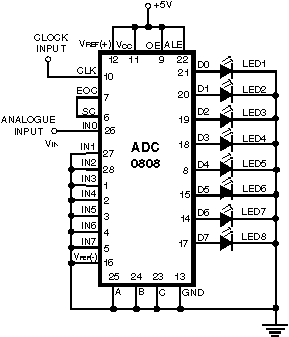
Simple Analog to Digital Converter (ADC)
Normally, an analog-to-digital converter (ADC) requires interfacing through a chip to convert analog signals into digital format. This necessitates both hardware and software, resulting in increased complexity and overall cost. The circuit presented here is configured around the ADC 0808,...
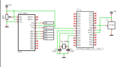
Analog To Digital Converter
An Analog-to-Digital Converter (ADC) is a circuit integrated into a single chip designed to convert analog signals into digital signals. Typically, an 8-bit ADC chip converts an analog signal ranging from 0 to 5 volts into a digital level ranging...
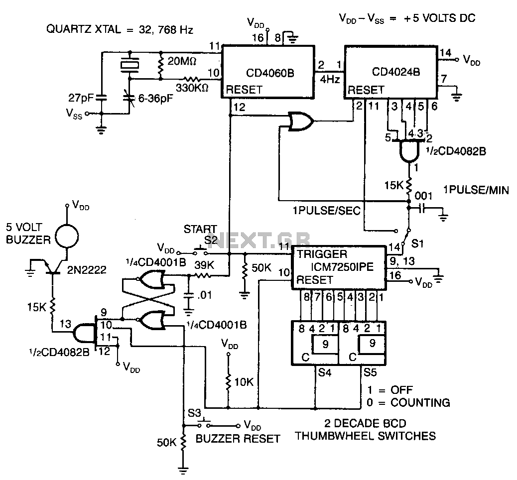
Cmos-precision-programmable-laboratory-timer
The time base is initially selected with switch S1 set for either seconds or minutes. Subsequently, values from 0 to 99 are chosen using the two thumbwheel switches S4 and S5. Finally, pressing switch S2 starts the timer. At the...
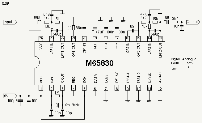
Digital Delay Unit For Surround Sound
The digital delay presented here is expected to be sufficient for most applications, and although the delay is fixed at 20ms, this is the most usable delay period. This is the equivalent of being about 7 metres away from the...
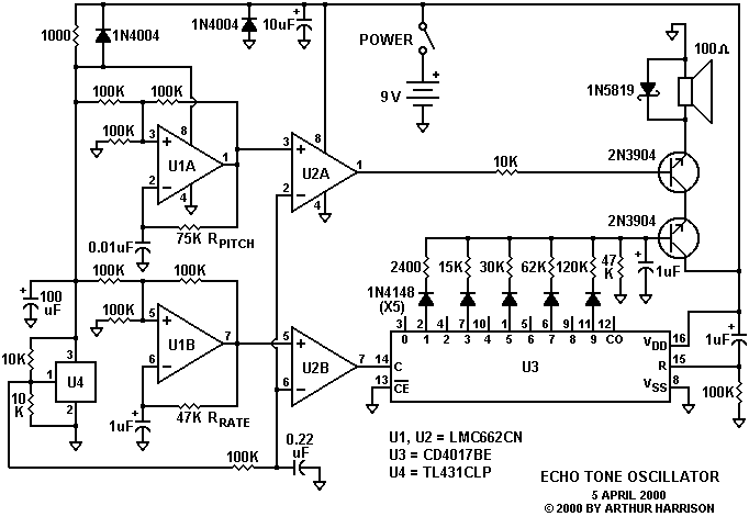
Echo Tone Oscillator
This simple circuit amplitude-modulates a single tone to approximate the echo effect similar to that produced by sonar apparatus. Individuals familiar with sonar-equipped vessels may recognize the imaginative similarities between this basic scheme and actual sonar technology. This circuit can...
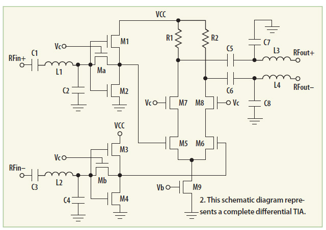
design cdba 018 m cmos
The design of a current difference buffer amplifier (CDBA) circuit for fabrication in a commercial CMOS semiconductor process allows for the versatile application of this component across various uses.
The current difference buffer amplifier (CDBA) is a specialized analog circuit that...
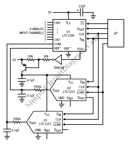
Autoranging Circuit
To extend the measurement range of an available ADC (analog to digital converter), autoranging can be utilized. If implemented on multiplexed input, this...
Autoranging is a technique employed in electronic measurement systems to automatically adjust the range of an analog-to-digital converter...
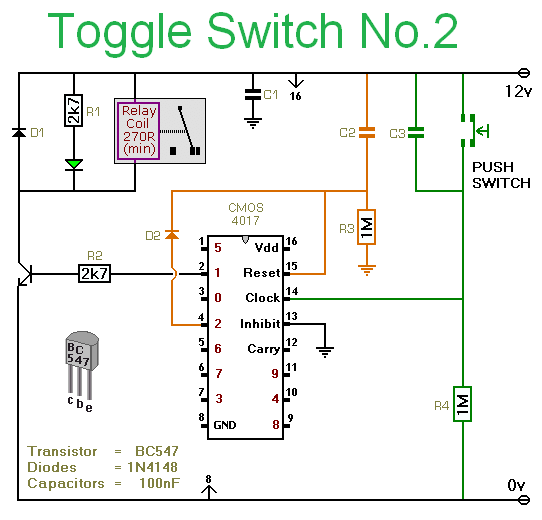
How To Use A Cmos 4017 As A Toggle Switch
This circuit utilizes a CMOS 4017 decade counter, which begins counting from zero and advances by one each time pin 14 is activated. Upon reaching nine, the count resets to zero and starts over. As the count progresses, each output...
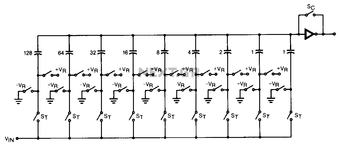
Switched-capacitor-adc
The CMOS comparator in the successive-approximation system determines each bit by examining the charge on a series of binary-weighted capacitors. In the first phase of the conversion process, the analog input is sampled by closing switch SC and all ST...