


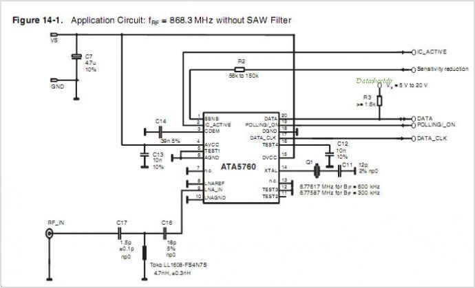
ATA5760 ATA5760 UHF ASK/FSK Receiver
#UHF
#ASK/FSK
#receiver
#high-power motors
#Gate driver
#Power MOSFETs
#full-bridge
#Charge Pump
#automotive applications
Description: The ATA6823 is designed specifically for automotive applications that require high-power motors. It provides four high-current gate driver outputs capable of driving a wide range of n-channel power MOSFETs in a full-bridge configuration. A fully integrated charge pump with external capacitors supplies the gate voltage for the high-side output stages. The ATA6823 supports low-speed LIN data communication up to 20 kBaud in compliance with LIN specification 2.0, utilizing a built-in LIN transceiver. Protection features include undervoltage and overvoltage detection with shutdown, overtemperature shutdown, and short circuit detection of motor leads to battery voltage and ground. Shoot-through protection is ensured through dead-time adjustment, which can be set by hardware. The ATA6823 application board enables the operation of a DC motor with a supply voltage ranging from 8V to 18V. The maximum power of the DC motor is constrained by the external H-bridge MOSFETs. No microcontroller is implemented on the board, allowing motor control either via an external microcontroller (with or without LIN bus) or directly using the DIR and PWM pins.
The ATA6823 integrated circuit is a robust solution for automotive applications that involve high-power motor control. Its architecture features four high-current gate driver outputs, which are essential for controlling n-channel power MOSFETs configured in a full-bridge arrangement. This configuration allows for efficient bidirectional control of the motor, making it suitable for various automotive applications such as electric power steering, window lifts, and other motor-driven systems.
The integrated charge pump is a noteworthy feature of the ATA6823, as it provides the necessary gate voltage for the high-side MOSFETs. This is crucial for ensuring that the MOSFETs operate effectively and can handle the high currents required in automotive environments. The use of external capacitors allows flexibility in design, enabling the selection of capacitance values that suit specific application requirements.
Communication capabilities are enhanced by the built-in LIN transceiver, which supports low-speed LIN data transmission up to 20 kBaud. This feature ensures compliance with LIN specification 2.0, facilitating communication between the motor control system and other automotive systems. This is particularly beneficial for applications requiring integration with existing vehicle networks.
The ATA6823 also incorporates several protection mechanisms to enhance reliability and safety. Undervoltage and overvoltage detection circuits monitor the supply voltage, triggering shutdowns to prevent damage to the device and the motor. The overtemperature shutdown feature protects the system from thermal overload, while short circuit detection safeguards against faults that could occur in the motor leads.
Shoot-through protection is a critical aspect of the ATA6823's design, preventing simultaneous conduction of high-side and low-side MOSFETs, which could lead to excessive current draw and potential damage. The dead-time adjustment feature offers a hardware-based solution for fine-tuning the switching intervals, ensuring optimal performance and reliability.
The application board for the ATA6823 is designed to facilitate the practical implementation of a DC motor control system. It operates with a supply voltage between 8V and 18V, accommodating a wide range of automotive power systems. The maximum power output is determined by the external H-bridge MOSFETs, which must be selected based on the specific motor requirements.
Control of the motor can be achieved through two primary methods: using an external microcontroller, which can be connected via the LIN bus for communication, or through direct control using the DIR (direction) and PWM (pulse-width modulation) pins. This flexibility allows engineers to design systems that meet the unique demands of their applications while leveraging the capabilities of the ATA6823 for efficient motor control.ATA6823 is designed specifically for automotive applications that require high-power motors. It provides four high-current Gate driver outputs capable of driving a wide range of n-channel Power MOSFETs in a full-bridge configuration. A fully integrated Charge Pump with external capacitors provides the Gate voltage for the high-side output stages.
ATA6823 supports low-speed LIN-data Communication up to 20 kBaud in compliance with LIN specification 2. 0 using a built-in LIN transceiver. Protection features include undervoltage/overvoltage detection and shutdown, overtemperature shutdown, and short circuit detection of motor leads to battery voltage and to ground.
Shoot-through protection is guaranteed using a dead-time adjustment which CAN be set by hardware. 2. Application Board The ATA6823 application board allows the running of a DC motor. The supply voltage is 8V to 18V, maximum power of the DC motor is limited by the external H-bridge MOSFETs No Microcontroller is implemented on-board. It is possible to control the motor either via an external Microcontroller (with or without LIN bus), or directly (using the DIR and PWM pins).
The ATA6823 integrated circuit is a robust solution for automotive applications that involve high-power motor control. Its architecture features four high-current gate driver outputs, which are essential for controlling n-channel power MOSFETs configured in a full-bridge arrangement. This configuration allows for efficient bidirectional control of the motor, making it suitable for various automotive applications such as electric power steering, window lifts, and other motor-driven systems.
The integrated charge pump is a noteworthy feature of the ATA6823, as it provides the necessary gate voltage for the high-side MOSFETs. This is crucial for ensuring that the MOSFETs operate effectively and can handle the high currents required in automotive environments. The use of external capacitors allows flexibility in design, enabling the selection of capacitance values that suit specific application requirements.
Communication capabilities are enhanced by the built-in LIN transceiver, which supports low-speed LIN data transmission up to 20 kBaud. This feature ensures compliance with LIN specification 2.0, facilitating communication between the motor control system and other automotive systems. This is particularly beneficial for applications requiring integration with existing vehicle networks.
The ATA6823 also incorporates several protection mechanisms to enhance reliability and safety. Undervoltage and overvoltage detection circuits monitor the supply voltage, triggering shutdowns to prevent damage to the device and the motor. The overtemperature shutdown feature protects the system from thermal overload, while short circuit detection safeguards against faults that could occur in the motor leads.
Shoot-through protection is a critical aspect of the ATA6823's design, preventing simultaneous conduction of high-side and low-side MOSFETs, which could lead to excessive current draw and potential damage. The dead-time adjustment feature offers a hardware-based solution for fine-tuning the switching intervals, ensuring optimal performance and reliability.
The application board for the ATA6823 is designed to facilitate the practical implementation of a DC motor control system. It operates with a supply voltage between 8V and 18V, accommodating a wide range of automotive power systems. The maximum power output is determined by the external H-bridge MOSFETs, which must be selected based on the specific motor requirements.
Control of the motor can be achieved through two primary methods: using an external microcontroller, which can be connected via the LIN bus for communication, or through direct control using the DIR (direction) and PWM (pulse-width modulation) pins. This flexibility allows engineers to design systems that meet the unique demands of their applications while leveraging the capabilities of the ATA6823 for efficient motor control.ATA6823 is designed specifically for automotive applications that require high-power motors. It provides four high-current Gate driver outputs capable of driving a wide range of n-channel Power MOSFETs in a full-bridge configuration. A fully integrated Charge Pump with external capacitors provides the Gate voltage for the high-side output stages.
ATA6823 supports low-speed LIN-data Communication up to 20 kBaud in compliance with LIN specification 2. 0 using a built-in LIN transceiver. Protection features include undervoltage/overvoltage detection and shutdown, overtemperature shutdown, and short circuit detection of motor leads to battery voltage and to ground.
Shoot-through protection is guaranteed using a dead-time adjustment which CAN be set by hardware. 2. Application Board The ATA6823 application board allows the running of a DC motor. The supply voltage is 8V to 18V, maximum power of the DC motor is limited by the external H-bridge MOSFETs No Microcontroller is implemented on-board. It is possible to control the motor either via an external Microcontroller (with or without LIN bus), or directly (using the DIR and PWM pins).
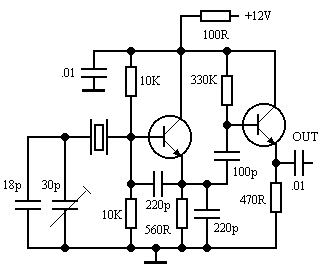
80M
This 80M receiver design incorporates the necessary switching mechanisms to enable the SSB filter and first intermediate frequency (I.F.) amplifier to function for transmission purposes. The receiver stages, from the radio frequency (R.F.) input to the speaker output, will be...
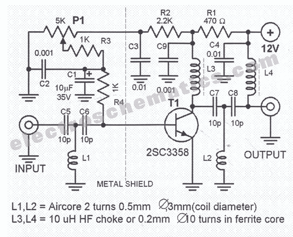
Wideband DTV UHF Antenna TV Amplifier Circuit using transistor 2sc3358
This HD TV UHF wideband amplifier (Ultra High Frequency amplifier) provides a total gain of 10 to 15 dB within the frequency range of 400 to 850 MHz, making it suitable for areas with weak television signals. To ensure optimal...
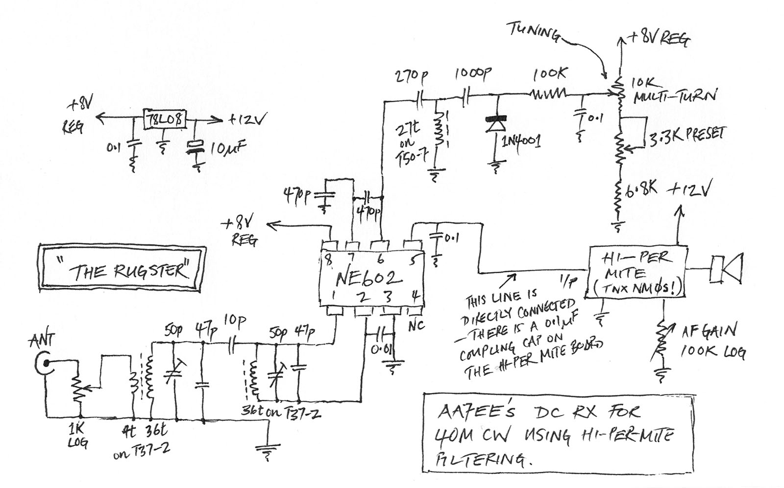
A Simple 80M Direct Conversion Receiver
A few weeks ago, Jason NT7S mentioned the ZL2BMI DSB transceiver as a rig that might be of interest for building. He was correct; it had been seen in SPRAT, but for some reason, it had not been seriously considered...
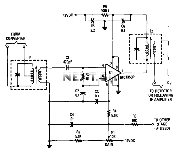
Receiver If Amplifier
Tl is tuned to the converter output frequency Ul to provide a gain of 45 to 50 dB, depending on the design of Tl and T2. C2, C3, C4, C5, and C6 function as bypass capacitors. R5 serves as a...
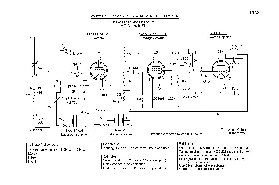
Battery Powered Tube Regenerative Receiver
The basic regenerative design is quite common. Before the schematic is created, there is a "concept stage," followed by the "available components stage," returning to the "concept stage," then moving on to the "mechanical/electrical layout stage," and finally sketching a...
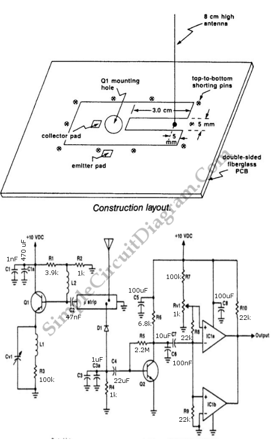
UHF Doppler Motion Detector
The UHF motion detector operates on the Doppler radar principle. An oscillating signal is generated by the oscillator (Q1), and a portion of this energy is reflected back.
The UHF motion detector employs the Doppler radar principle to detect motion through...

6-17 MHz SW reciever
Its very simple as It uses only 3 transistors 2n2222. The Coils can be altered to change the range of reception by lowering or highering the frequency. More: This circuit is a SW band receiver of range 6 to 17...
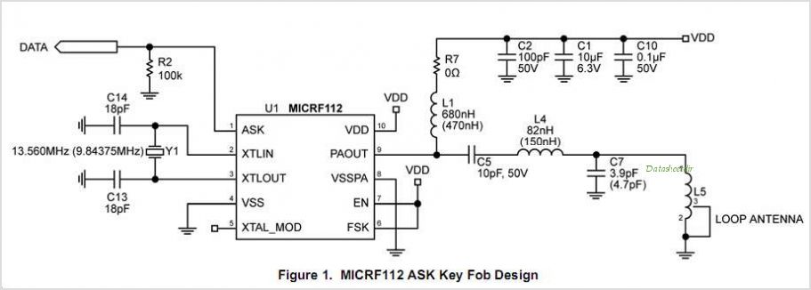
MICRF112 MICRF112: QwikRadio ?® UHF ASK/FSK Transmitter
The ADC12038 family consists of 12-bit plus sign sampling Analog-to-Digital Converters (ADCs) featuring serial input/output. These devices are equipped with configurable analog multiplexers that can accommodate 2, 4, or 8 input channels. Upon request, these ADCs can execute a self-calibration...
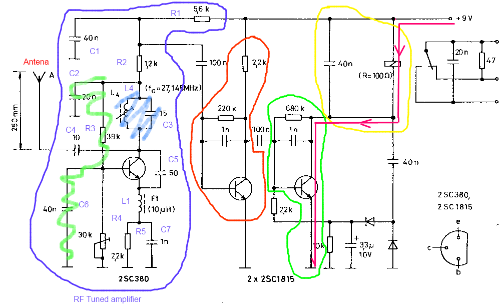
signal Can someone break down how this receiver works
The circuit described is a toy car receiver, which operates similarly to the transmitter but in reverse and with additional filtering. The receiver is tuned to a frequency of 27.145 MHz to capture signals at this frequency. Following the initial...