


Using LVDS serializer/deserializer devicesm
#LVDS
#serializer
#deserializer
#Maxim Integrated
#digital video
#signal transmission
#STP cable
#data stream
#low voltage
#differential signaling
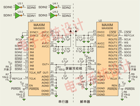
Description: Low Voltage Differential Signaling (LVDS) is an effective digital video signal transmission interface that supports low-cost digital audio data streaming. This article discusses the use of Maxim Integrated Products Inc.'s MAX9205/MAX9206 10-bit LVDS serializer/deserializer (SerDes) to transmit up to four I2S audio data streams via STP cable. Maintaining audio signals in digital form is crucial for achieving optimal sound quality, as conversions between analog and digital domains can degrade quality. While the Media Oriented Systems Transport (MOST) bus is designed for audio data transmission in vehicles, it is often more expensive to implement. For consumer audio equipment, the S/PDIF interface is commonly used for transmitting compressed audio data between devices, but it lacks the bandwidth for uncompressed 5.1 or 7.1 digital audio formats. LVDS provides a robust, low-cost, high-bandwidth solution for digital audio data transmission that can be integrated into existing hardware without straining system resources. By keeping audio data digital, the need for multiple ADCs, DACs, and cables is eliminated, thus saving costs and board space for other functionalities. LVDS is already utilized in transmitting video data from cameras, DVD players, and navigation systems to various display devices in vehicles. The low signal amplitude and differential structure of LVDS minimize electromagnetic radiation during high-bandwidth data transmission. The MAX9205 is designed to transmit a single reference clock along with 10-bit parallel data. I2S signals utilize SCLK, WS, and SDA0-3 for data reference clock and synchronization, with SCLK operating at least twice the frequency of the reference clock. The reference clock frequency for the MAX9205 ranges from 16 to 40 MHz, but the chip locks down to 10 MHz, allowing the use of a common clock frequency of 12.28 MHz. The module is robust enough to endure harsh automotive environments. The LVDS bus requires AC coupling to prevent high voltage in case of short circuits. Since the MAX9205 does not automatically output DC-balanced signals, it is essential to ensure that the transmitted data is DC-balanced. Out of the 10 available inputs, typically no more than six are used, allowing the remaining four inputs to assist with DC balancing. The WS signal is symmetric to the SCLK signal, so only the random signals SDA0-3 should be fed to the unused inputs to ensure that each dual-channel I2S packet contains an equal number of 1s and 0s. To avoid excessive jitter in the MAX9206 deserializer output, I2S signals should not change state during sampling. The TCLK_R/F should be connected to ground, allowing the MAX9205 reference clock (TCLK) to sample on the falling edge. It is assumed that the SCLK state changes on the rising edge of TCLK. If adjustments are necessary, TCLK_R/F should be modified to ensure that the input signal meets the timing requirements. Waveform samples for the I2S input signal are illustrated in Figure 1, while Figure 2 provides the application schematic for the MAX9205 and MAX9206. The left section of the schematic includes the circuitry required for sending LVDS serial audio data streams, while the right section encompasses the SerDes circuit.
The LVDS interface is particularly advantageous in automotive applications due to its ability to transmit high-quality audio data over long distances with minimal interference. The differential signaling used in LVDS reduces the susceptibility to noise, making it suitable for environments with significant electromagnetic interference. The implementation of the MAX9205/MAX9206 SerDes allows for efficient data handling, ensuring that audio streams maintain integrity from source to destination.
In practical applications, the integration of the MAX9205 and MAX9206 into automotive systems can lead to enhanced audio experiences, allowing for features such as surround sound and high-fidelity playback. The design considerations for the implementation should include proper layout techniques to minimize crosstalk and ensure signal integrity. Additionally, attention should be given to the power supply design, as fluctuations in power can affect the performance of the LVDS system.
Overall, the LVDS interface, particularly with the MAX9205/MAX9206 components, represents a robust solution for modern automotive audio systems, combining high performance with cost-effectiveness and ease of integration into existing architectures. This makes it a preferred choice for manufacturers aiming to deliver superior audio quality in vehicles.Low Voltage Differential Signaling (LVDS) interface is a digital video signal transmission vehicle of the most effective interface, it is to send digital audio data stream of low-cost program. This article describes how the use of Maxim Integrated Products Inc. (Maxim) The MAX9205/MAX9206 10 bit LVDS serializer / deserializer (SerDes), through the STP cable to send up to four I2S audio data streams. Domain audio signal in analog and digital domains will reduce the quality of each conversion, so as far as possible for the audio data in digital form to get the best sound quality is very important. Transmission-oriented media system (MOST) bus for audio data transmission and vehicle design, but more expensive to implement, andfor most applications.
For consumer audio equipment, generally use S / PDIF (by SONY and PHILIPS companies co-developed a digital audio output interface) to compressed audio data transmitted from an audio device to another audio device. However, S / PDIF not be sufficient bandwidth to send uncompressed format 5. 1 or 7. 1 digital audio, but also suitable for automotive applications, the lack of a proven, robust physical layer.
The use of LVDS transmission of digital audio data is a robust, low-cost, high-bandwidth interface options that can easily be added to existing hardware, without affecting system resources. Is now available I2S digital audio data can be transferred to different parts of cars, but not actually on the software overhead.
By maintaining the audio data in digital form, the system no longer require multiple ADC, DAC and cables, which saved the cost and board space can be used to achieve other functions. LVDS has been used to from the camera, DVD player and navigation system, video data sent to the vehicle routing in a variety of display devices.
LVDS available low signal amplitude and differential structure in order to allow it to electromagnetic radiation is very low high-bandwidth data transmission. MAX9205 has been designed to send a single reference clock 10-bit parallel data. I2S signals for SCLK, WS and SDA0-3 as a data reference clock and synchronization with the SCLK at least 2 times its frequency.
MAX9205 requirements for the reference clock frequency range 16 ~ 40MHz, but the chip reference clock will be locked down to 10MHz, thus allowing the use of commonly used clock frequency of 12. 28MHz. Leave the module in the signal beam line to be very robust, able to endure the harsh automotive environment and state failure.
LVDS bus need to be AC-coupled, so as to avoid high pressure in the event of damage to short-circuit situation. Since the MAX9205 does not automatically signal to the output DC-balanced, it should be to ensure that the data to be transmitted has been DC-balanced.
10 available in the input, generally not used more than six, it can make use of the remaining four input data for the transmission of DC-balanced. And WS-signal SCLK signal is symmetric, so only on the random signal SDA0-3 to RP and feed to the unused input to be sent to ensure that dual-channel I2S each packet equal to the number of 1 and 0.
To meet the establishment and maintenance of the MAX9205 time and prevent the MAX9206 deserializer output jitter is too large, it should be in the I2S signals change state is not in its sample. Will TCLK_R / F access to GND, so that in the MAX9205 reference clock (TCLK) falling edge of the input sample.
It is assumed that the state of the SCLK rising edge of TCLK to change. If the configuration, it is necessary to TCLK_R / F be adjusted as appropriate to ensure that the input signal to meet the time requirements to establish and maintain. Right I2S input signal waveform samples shown in figure 1. Figure 2 gives the MAX9205 and MAX9206 application schematic. Left part of the serial circuit includes sending LVDS serial and audio data streams required for the circuit.
Right part of the SerDes circuit includes r
The LVDS interface is particularly advantageous in automotive applications due to its ability to transmit high-quality audio data over long distances with minimal interference. The differential signaling used in LVDS reduces the susceptibility to noise, making it suitable for environments with significant electromagnetic interference. The implementation of the MAX9205/MAX9206 SerDes allows for efficient data handling, ensuring that audio streams maintain integrity from source to destination.
In practical applications, the integration of the MAX9205 and MAX9206 into automotive systems can lead to enhanced audio experiences, allowing for features such as surround sound and high-fidelity playback. The design considerations for the implementation should include proper layout techniques to minimize crosstalk and ensure signal integrity. Additionally, attention should be given to the power supply design, as fluctuations in power can affect the performance of the LVDS system.
Overall, the LVDS interface, particularly with the MAX9205/MAX9206 components, represents a robust solution for modern automotive audio systems, combining high performance with cost-effectiveness and ease of integration into existing architectures. This makes it a preferred choice for manufacturers aiming to deliver superior audio quality in vehicles.Low Voltage Differential Signaling (LVDS) interface is a digital video signal transmission vehicle of the most effective interface, it is to send digital audio data stream of low-cost program. This article describes how the use of Maxim Integrated Products Inc. (Maxim) The MAX9205/MAX9206 10 bit LVDS serializer / deserializer (SerDes), through the STP cable to send up to four I2S audio data streams. Domain audio signal in analog and digital domains will reduce the quality of each conversion, so as far as possible for the audio data in digital form to get the best sound quality is very important. Transmission-oriented media system (MOST) bus for audio data transmission and vehicle design, but more expensive to implement, andfor most applications.
For consumer audio equipment, generally use S / PDIF (by SONY and PHILIPS companies co-developed a digital audio output interface) to compressed audio data transmitted from an audio device to another audio device. However, S / PDIF not be sufficient bandwidth to send uncompressed format 5. 1 or 7. 1 digital audio, but also suitable for automotive applications, the lack of a proven, robust physical layer.
The use of LVDS transmission of digital audio data is a robust, low-cost, high-bandwidth interface options that can easily be added to existing hardware, without affecting system resources. Is now available I2S digital audio data can be transferred to different parts of cars, but not actually on the software overhead.
By maintaining the audio data in digital form, the system no longer require multiple ADC, DAC and cables, which saved the cost and board space can be used to achieve other functions. LVDS has been used to from the camera, DVD player and navigation system, video data sent to the vehicle routing in a variety of display devices.
LVDS available low signal amplitude and differential structure in order to allow it to electromagnetic radiation is very low high-bandwidth data transmission. MAX9205 has been designed to send a single reference clock 10-bit parallel data. I2S signals for SCLK, WS and SDA0-3 as a data reference clock and synchronization with the SCLK at least 2 times its frequency.
MAX9205 requirements for the reference clock frequency range 16 ~ 40MHz, but the chip reference clock will be locked down to 10MHz, thus allowing the use of commonly used clock frequency of 12. 28MHz. Leave the module in the signal beam line to be very robust, able to endure the harsh automotive environment and state failure.
LVDS bus need to be AC-coupled, so as to avoid high pressure in the event of damage to short-circuit situation. Since the MAX9205 does not automatically signal to the output DC-balanced, it should be to ensure that the data to be transmitted has been DC-balanced.
10 available in the input, generally not used more than six, it can make use of the remaining four input data for the transmission of DC-balanced. And WS-signal SCLK signal is symmetric, so only on the random signal SDA0-3 to RP and feed to the unused input to be sent to ensure that dual-channel I2S each packet equal to the number of 1 and 0.
To meet the establishment and maintenance of the MAX9205 time and prevent the MAX9206 deserializer output jitter is too large, it should be in the I2S signals change state is not in its sample. Will TCLK_R / F access to GND, so that in the MAX9205 reference clock (TCLK) falling edge of the input sample.
It is assumed that the state of the SCLK rising edge of TCLK to change. If the configuration, it is necessary to TCLK_R / F be adjusted as appropriate to ensure that the input signal to meet the time requirements to establish and maintain. Right I2S input signal waveform samples shown in figure 1. Figure 2 gives the MAX9205 and MAX9206 application schematic. Left part of the serial circuit includes sending LVDS serial and audio data streams required for the circuit.
Right part of the SerDes circuit includes r
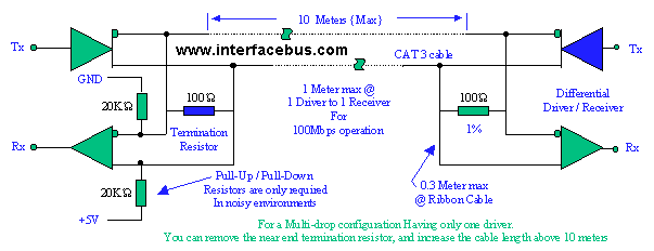
Bus Description RS644 LVDS
The circuit is designed to provide an output voltage swing of 350 mV at speeds exceeding 400 Mbps into a 100-ohm load over a distance of approximately 10 meters. Low-Voltage Differential Signaling (LVDS) is an electrical specification that serves as...
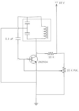
Simple low voltage Oscillator circuit
The frequency remains stable as the voltage decreases. It is referred to as the "backwards JT" because it operates optimally with a bifilar coil and a single transistor. With a modification to the circuit, it is possible to deplete a...
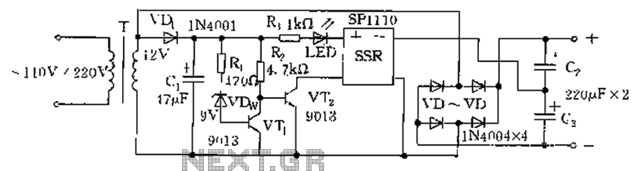
Schematic circuit diagram of low voltage and low voltage automatic conversion
The circuit is automatically converted to a low-voltage configuration. A 220V AC supply is stepped down by transformer T. After this, the breakdown voltage of diode VDw causes transistors VT1 and VT2 to turn off, resulting in the solid-state relay...
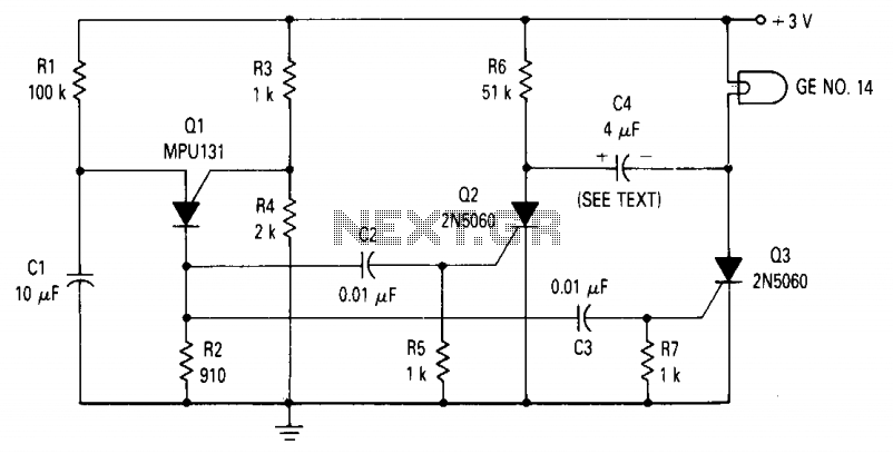
Low voltage lamp flasher
The circuit consists of a relaxation oscillator created by Q1 and an SCR flip-flop formed by Q2 and Q3. When the supply voltage is applied to the circuit, the timing capacitor C1 charges to the firing point of the Programmable...
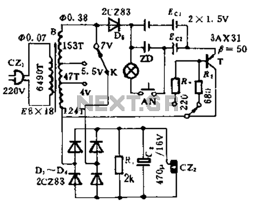
Low voltage DC power charger circuit
This circuit is designed for high current applications using nickel-cadmium rechargeable batteries, and it can also function as a general low-voltage DC power supply. The circuit consists of a charging section and a DC output section. K2 serves as the...
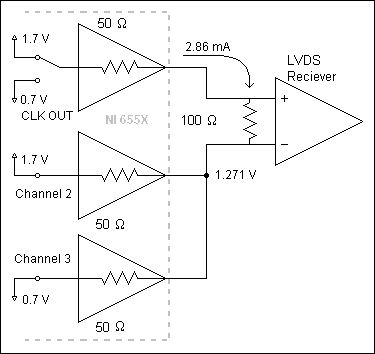
Interfacing to LVDS with the NI 655X Digital Waveform Generator/Analyzer
The NI 655X is a versatile high-speed digital product capable of interfacing with various technologies. This application note illustrates how to connect the NI 655X to Low Voltage Differential Signaling (LVDS) devices. LVDS is an emerging differential digital standard utilized...
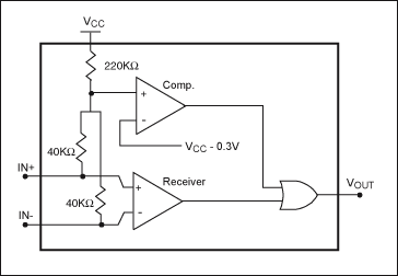
Understanding LVDS Fail-Safe Circuits
The LVDS receiver requires a failsafe function to prevent an uncertain output state in the event of an improper connection. This application note explores the circuits and characteristics of three common failsafe functions: external biasing, in-path, and parallel.
The LVDS (Low-Voltage...
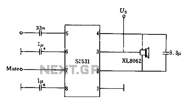
The battery voltage is low frequency amplifying circuit diagram 1v
The battery voltage is 1V for a low-frequency amplifying circuit, which can operate with a power supply voltage ranging from 1V to 1.7V, making it suitable for use with small batteries. The circuit provides an output power of 80mW with...
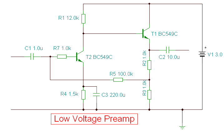
Low Voltage Preamplifier
This is a specialized low-voltage version of an audio preamplifier. The emitter voltage of transistor T1 is biased close to half the supply voltage (1.5V) to enable maximum output voltage swing. Both transistors are directly coupled and utilize closed-loop feedback...