Hot Swapping the PCI Bus
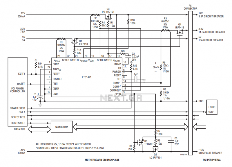
Sense resistors R1, R2 and R3 provide current fault protection. When the voltage across R1 and R2 is greater than 50mV for more than 10μs, the LTC1421 circuit breaker is tripped. All of the FETs are immediately turned off and the FAULT pin is pulled low. The circuit breaker is reset by cycling the POR pin. The current fault protection for the 3.3V supply is provided by resistive divider R6 and R8 and the uncommitted comparator in the LTC1421. Because the current levels on the –12V supply are so low, overcurrent protection is not necessary. The QuickSwitch bus switch contains a low resistance N-channel placed in series with the data bus. The switch is turned off when the board is inserted and then enabled after the power is stable. The switch inputs and outputs do not have a parasitic diode back to VCC and have very low capacitance. System Timing The system timing is shown in Figure 2. The PCI power controller senses when a board has been inserted into the PCI via the power-select bits. Alternatively, the user can inform the controller that a board has been inserted via a front panel or keyboard. The PCI controller holds the RST# pin low and disables the QuickSwitch bus switches, then turns on the LTC1421 via the POR pin. The power supplies turn on at a controlled rate and when the 12V supply is within 10% of its final value, the PWRGD signal pulls high. The PCI power controller waits one reset time-out period and then pulls RST# high and enables the QuickSwitch devices.
The circuitry described operates to ensure the safe and efficient management of power supplies in a hot-swappable PCI environment. The LTC1421 serves as a power management integrated circuit (PMIC), coordinating the operation of the external N-channel pass transistors (Q1-Q4) which regulate the 12V, 5V, 3.3V, and -12V supplies. The controlled ramping of these voltages mitigates the risk of inrush current, which could otherwise damage components or lead to system instability. The ramp rate is critical, particularly for the positive voltage supplies, which are calculated based on the capacitance in the circuit, facilitating a gradual increase in voltage.
Current fault protection is implemented through the use of sense resistors (R1, R2, R3) which monitor the voltage drop across them. If the voltage exceeds a predetermined threshold, the LTC1421 activates its internal circuit breaker mechanism, immediately disabling the associated FETs to prevent damage from overcurrent conditions. This is particularly important in applications where power integrity is crucial.
The QuickSwitch bus switches play a vital role in managing the data bus connections. By being disabled during the initial power-up sequence, they prevent any data corruption or erroneous signals while the power supplies stabilize. The absence of parasitic diodes in the switch design further enhances reliability, ensuring that no unintended paths for current exist that could interfere with the operation of the system.
Timing for the power-up sequence is carefully controlled, with the PCI controller managing the state of the RST# pin and ensuring that the system only transitions to an operational state once all power supplies are stable and within acceptable limits. This comprehensive approach to power management and fault protection is essential for maintaining the reliability and functionality of hot-swappable PCI slots in modern computing systems.The circuitry for a hot swappable PCI slot on a motherboard or backplane is shown in Figure 1. The power supplies for each PCI slot are controlled by an LTC1421 and four external FETs, and the data bus is buffered by several QS3384 QuickSwitches or equivalent. A PCI power control ASIC, FPGA, microprocessor or the like, controls all of the slots within the system.
The 12V, 5V, 3.3V and – 12V supplies are controlled by placing external N-channel pass transistors, Q1 to Q4, in the power path. By increasing the voltage on the gate of the pass transistors at a controlled rate, the transient surge current (I = C • dV/dt) drawn from the PCI supplies can be limited to a safe value.
The ramp rate for the positive supplies is set by dV/dt = 20μA/C2. The –12V supply ramp rate is set by R7 and C3, while resistor R5 and transistor Q5 help turn off transistor Q2 quickly. Resistors R9, R11 and R12 prevent potential high frequency FET oscillations. Resistors R13 and R14 pull up PWRGD and FAULT to the proper logic level.
Sense resistors R1, R2 and R3 provide current fault protection. When the voltage across R1 and R2 is greater than 50mV for more than 10μs, the LTC1421 circuit breaker is tripped. All of the FETs are immediately turned off and the FAULT pin is pulled low. The circuit breaker is reset by cycling the POR pin. The current fault protection for the 3.3V supply is provided by resistive divider R6 and R8 and the uncommitted comparator in the LTC1421.
Because the current levels on the –12V supply are so low, overcurrent protection is not necessary. The QuickSwitch bus switch contains a low resistance N-channel placed in series with the data bus. The switch is turned off when the board is inserted and then enabled after the power is stable. The switch inputs and outputs do not have a parasitic diode back to VCC and have very low capacitance.
System Timing The system timing is shown in Figure 2. The PCI power controller senses when a board has been inserted into the PCI via the power-select bits. Alternatively, the user can inform the controller that a board has been inserted via a front panel or keyboard.
The PCI controller holds the RST# pin low and disables the QuickSwitch bus switches, then turns on the LTC1421 via the POR pin. The power supplies turn on at a controlled rate and when the 12V supply is within 10% of its fi nal value, the PWRGD signal pulls high.
The PCI power controller waits one reset time-out period and then pulls RST# high and enables the QuickSwitch devices.