


ZX Interface 2
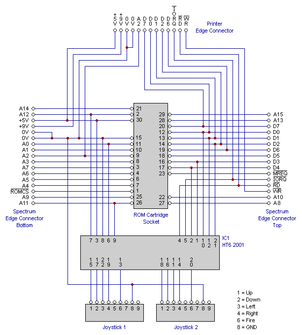
Description: The circuitry of the ZXInterface2 is straightforward, consisting of a single custom-made integrated circuit (IC) that handles address decoding for the dual joystick interface. The ROM cartridge socket provides access to signals already present at the Spectrum's edge connector. Photographs of the printed circuit board (PCB) indicate that at least two versions of the board were produced. However, the Service Manual states that no modifications were made to the ZXInterface2 design, suggesting that only the second version was commercially available. The pinout for the ROM cartridge slot is detailed below. It is important to note that the contacts of both the socket and each ROM cartridge are gold-plated to ensure a more reliable electrical connection. When a ROM cartridge is inserted, it connects the /ROMCS (ROM Chip Select) line directly to the 5V line, thereby disabling the Spectrum's ROM and allowing the cartridge's ROM to occupy the 0 - 16384 memory map area. The cartridge's ROM is designed to output data to the data bus only when the lower 16K of memory is accessed. During this access, the address lines A14 and A15, along with the /MREQ (Memory REQuest) line, will all be at logic 0. These three lines are utilized within the cartridge to enable its ROM. Address lines A0 - A13 indicate a specific location within the ROM, and the data from that location is output on lines D0 - D7. It should be noted that the /RD (ReaD) and /WR (WRite) signals available at the Spectrum's edge connector are not present at the ROM cartridge slot. Consequently, all read and write operations to the ROM are treated as memory reads. This design choice is advantageous as ROMs are inherently read-only devices, eliminating the need for write capabilities. This design reduces the size of the ROM cartridge socket and simplifies the required decoding circuitry. However, it also implies that a cartridge containing both 8K ROM and 8K RAM is unfeasible due to the absence of a write mechanism for the RAM. Moreover, since the /RD and /WR signals are disregarded, the ROM can be accessed during the memory refresh cycle when the /RFSH signal is low. A ROM cartridge consists of a compact double-sided PCB with a 16K ROM chip mounted on it. The ROM is not encased in a standard DIL pin package; instead, bare silicon is utilized to minimize the size and manufacturing cost of the ROM cartridge. The diagram below illustrates how the 16K ROM might appear if it were housed in a DIL pin package, aiding in understanding the address decoding process within the cartridge. Although not depicted in the diagram, address lines A0 - A13 and data lines D0 - D7 at the ROM cartridge socket connect to the corresponding pins on the ROM. The A14 line connects to the ROM's /CE (Chip Enable) pin, which must be held at logic 0 for the ROM to be selected. However, data is output from the ROM only when both the /OE1 (Output Enable 1) and /OE2 (Output Enable 2) pins are at logic 0. These two lines are controlled by /MREQ and A15, respectively. Thus, data output from the ROM occurs only during memory accesses where the upper two address lines are low, specifically when reading or writing to addresses 0 - 16383, corresponding to the lower 16K of the memory map. The pinout of the ROM cartridge socket closely resembles that of a standard 16K ROM IC. The design of the ROM cartridge significantly streamlines the circuitry and reduces the costs associated with the ZXInterface2. However, it does impose limitations on the capabilities of ROM cartridges. The Spectrum's ROM is always removed from the memory map when a ROM cartridge is connected, and there is no mechanism for paging between the two ROMs. Consequently, accessing routines within the Spectrum's ROM is impossible; such routines must be duplicated within the ROM cartridge, consuming valuable memory resources. Additionally, utilizing the features of the ZXInterface1, including Microdrive, Network, and RS232 functionalities, presents challenges.
The ZXInterface2 serves as an essential interface for the ZX Spectrum, enabling the use of external ROM cartridges for enhanced functionality. Its design philosophy prioritizes simplicity and cost-effectiveness, employing a single custom IC to manage the address decoding process. This architecture allows for straightforward integration with the existing hardware of the Spectrum, facilitating the connection of ROM cartridges that expand the system's capabilities.
The ROM cartridge socket's design, featuring gold-plated contacts, ensures reliable connections, which is critical for maintaining data integrity during operation. The decision to disable the Spectrum's internal ROM upon cartridge insertion is a strategic one, allowing developers to create software that can operate independently of the built-in ROM, but it also necessitates that any required routines be included within the cartridge itself.
The limitations of the ZXInterface2's design, particularly regarding the inability to access the Spectrum's ROM while a cartridge is in use, highlight the trade-offs involved in creating a streamlined interface. While the architecture simplifies the connection process and reduces component count, it restricts the versatility of the system, particularly for applications that require access to both the internal and external ROMs.
Overall, the ZXInterface2 exemplifies a balance between functionality and simplicity, making it a noteworthy component in the ZX Spectrum ecosystem while also illustrating the inherent challenges of designing flexible and capable hardware interfaces.The circuitry of the ZXInterface2 is very simple and is comprised of a single custom made IC which performs address decoding for the twin joystick interface. The ROM cartridge socket simply exposes signals already available from the Spectrum`s edge connector.
As can be seen from the P. C. B. photographs, at least two issues of the board were produce d. However, the Service Manual indicates that no modifications were made to the ZXInterface2 design and hence it is likely that only issue 2 versions were sold. The pinout of the ROM cartridge slot is shown below. Note that the contacts of the socket, and of each ROM cartridge, are gold plated to achieve a more reliable electrical connection.
When a ROM cartridge is plugged in, it connects the /ROMCS (ROM Chip Select) line directly to the 5V line. This disables the Spectrum`s ROM thereby allowing the cartridge`s ROM to appear in the 0 - 16384 memory map area.
The cartridge`s ROM must only output to the data bus when the lower 16K of memory is addressed. When an access to this memory area occurs, the address lines A14 and A15 and the /MREQ (Memory REQuest) line will all be at logic 0. These three lines are therefore used inside the cartridge to enable its ROM. Address lines A0 - A13 specify a location within the ROM and the data from that location is output on lines D0 - D7.
Note that the /RD (ReaD) and /WR (WRite) signals exposed at the edge connector of the Spectrum are not available at the ROM cartridge slot. As a result, both read and write accesses to the ROM will be treated as a memory read. This is not a problem as, by its very nature, a ROM is a read-only device and hence would not be written to.
This approach has the advantage that it reduces the size of the ROM cartridge socket but the main reason why it was adopted was to simplify the decoding circuitry required. It does however mean that a cartridge consisting of 8K ROM and 8K RAM is impossible as there is no mechanism for writing to the RAM.
Also since the /RD and /WR signals are ignored, the ROM can also be accessed during the memory refresh cycle when the /RFSH signal is low. A ROM cartridge consists a small double sided P. C. B. with a 16K ROM chip mounted on it. The ROM is not housed in a standard DIL pin package but instead just the bare silicon is used. This reduces the size and fabrication cost of the ROM cartridge. The diagram below shows the 16K ROM as it might appear if housed in a DIL pin package, and aids in understanding how address decoding is achieved within the cartridge.
Although not shown in the diagram, address lines A0 - A13 and data lines D0 - D7 at the ROM cartridge socket connect to the corresponding pins on the ROM. A14 connects to the ROM`s /CE (Chip Enable) pin. This pin must be held at logic 0 for the ROM to become selected. However, it is only when the ROM`s /OE1 (Output Enable 1) and /OE2 (Output Enable 2) pins are both at logic 0 that data is output from the ROM.
These two lines are driven by /MREQ and A15 respectively. Therefore only when a memory access is made with the upper two address lines held low will the ROM output data. This condition will only occur when reading (or writing) to addresses 0 - 16383, i. e. the lower 16K of the memory map. Note how the pinout of the ROM cartridge socket closely matches the pinout of a typical 16K ROM IC. The design of the ROM cartridge greatly simplifies the circuitry and cost of the ZXInterface2. However, it does limit the capability offered by ROM cartridges. The Spectrum`s ROM is always paged out of the memory map when a ROM cartridge is plugged in. There is no mechanism to allow paging between the two ROMs and hence it is impossible to access routines within the Spectrum`s ROM.
If such routines are required then they must be reproduced within the ROM cartridge, using up valuable memory space. Accessing the features of the ZXInterface1 (Microdrive, Network and RS232) is also difficult
The ZXInterface2 serves as an essential interface for the ZX Spectrum, enabling the use of external ROM cartridges for enhanced functionality. Its design philosophy prioritizes simplicity and cost-effectiveness, employing a single custom IC to manage the address decoding process. This architecture allows for straightforward integration with the existing hardware of the Spectrum, facilitating the connection of ROM cartridges that expand the system's capabilities.
The ROM cartridge socket's design, featuring gold-plated contacts, ensures reliable connections, which is critical for maintaining data integrity during operation. The decision to disable the Spectrum's internal ROM upon cartridge insertion is a strategic one, allowing developers to create software that can operate independently of the built-in ROM, but it also necessitates that any required routines be included within the cartridge itself.
The limitations of the ZXInterface2's design, particularly regarding the inability to access the Spectrum's ROM while a cartridge is in use, highlight the trade-offs involved in creating a streamlined interface. While the architecture simplifies the connection process and reduces component count, it restricts the versatility of the system, particularly for applications that require access to both the internal and external ROMs.
Overall, the ZXInterface2 exemplifies a balance between functionality and simplicity, making it a noteworthy component in the ZX Spectrum ecosystem while also illustrating the inherent challenges of designing flexible and capable hardware interfaces.The circuitry of the ZXInterface2 is very simple and is comprised of a single custom made IC which performs address decoding for the twin joystick interface. The ROM cartridge socket simply exposes signals already available from the Spectrum`s edge connector.
As can be seen from the P. C. B. photographs, at least two issues of the board were produce d. However, the Service Manual indicates that no modifications were made to the ZXInterface2 design and hence it is likely that only issue 2 versions were sold. The pinout of the ROM cartridge slot is shown below. Note that the contacts of the socket, and of each ROM cartridge, are gold plated to achieve a more reliable electrical connection.
When a ROM cartridge is plugged in, it connects the /ROMCS (ROM Chip Select) line directly to the 5V line. This disables the Spectrum`s ROM thereby allowing the cartridge`s ROM to appear in the 0 - 16384 memory map area.
The cartridge`s ROM must only output to the data bus when the lower 16K of memory is addressed. When an access to this memory area occurs, the address lines A14 and A15 and the /MREQ (Memory REQuest) line will all be at logic 0. These three lines are therefore used inside the cartridge to enable its ROM. Address lines A0 - A13 specify a location within the ROM and the data from that location is output on lines D0 - D7.
Note that the /RD (ReaD) and /WR (WRite) signals exposed at the edge connector of the Spectrum are not available at the ROM cartridge slot. As a result, both read and write accesses to the ROM will be treated as a memory read. This is not a problem as, by its very nature, a ROM is a read-only device and hence would not be written to.
This approach has the advantage that it reduces the size of the ROM cartridge socket but the main reason why it was adopted was to simplify the decoding circuitry required. It does however mean that a cartridge consisting of 8K ROM and 8K RAM is impossible as there is no mechanism for writing to the RAM.
Also since the /RD and /WR signals are ignored, the ROM can also be accessed during the memory refresh cycle when the /RFSH signal is low. A ROM cartridge consists a small double sided P. C. B. with a 16K ROM chip mounted on it. The ROM is not housed in a standard DIL pin package but instead just the bare silicon is used. This reduces the size and fabrication cost of the ROM cartridge. The diagram below shows the 16K ROM as it might appear if housed in a DIL pin package, and aids in understanding how address decoding is achieved within the cartridge.
Although not shown in the diagram, address lines A0 - A13 and data lines D0 - D7 at the ROM cartridge socket connect to the corresponding pins on the ROM. A14 connects to the ROM`s /CE (Chip Enable) pin. This pin must be held at logic 0 for the ROM to become selected. However, it is only when the ROM`s /OE1 (Output Enable 1) and /OE2 (Output Enable 2) pins are both at logic 0 that data is output from the ROM.
These two lines are driven by /MREQ and A15 respectively. Therefore only when a memory access is made with the upper two address lines held low will the ROM output data. This condition will only occur when reading (or writing) to addresses 0 - 16383, i. e. the lower 16K of the memory map. Note how the pinout of the ROM cartridge socket closely matches the pinout of a typical 16K ROM IC. The design of the ROM cartridge greatly simplifies the circuitry and cost of the ZXInterface2. However, it does limit the capability offered by ROM cartridges. The Spectrum`s ROM is always paged out of the memory map when a ROM cartridge is plugged in. There is no mechanism to allow paging between the two ROMs and hence it is impossible to access routines within the Spectrum`s ROM.
If such routines are required then they must be reproduced within the ROM cartridge, using up valuable memory space. Accessing the features of the ZXInterface1 (Microdrive, Network and RS232) is also difficult