


digital logic How to calculate Gate Delays in normal Adders and Carry Look Ahead Adders
#adder
#gate delay
#carry look ahead
#ripple adder
#4-bit adder
#logic design
#binary arithmetic
#digital circuits
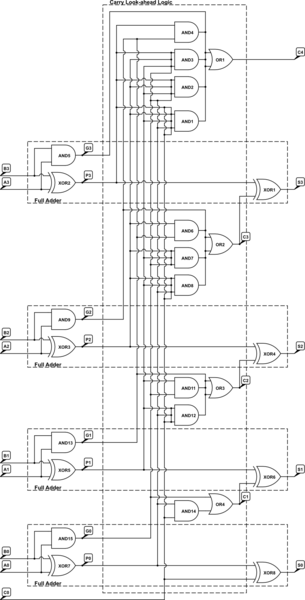
Description: A 4-bit Carry Look Ahead Adder has 3 gate delays for all carry bits and 4 gate delays for all sum bits, whereas ripple adders have 7 and 8 gate delays, respectively.
The 4-bit Carry Look Ahead Adder (CLA) is designed to improve the speed of binary addition by reducing the time required to calculate carry bits compared to traditional ripple carry adders. In a ripple carry adder, each carry bit must wait for the previous carry bit to be calculated, resulting in a cumulative delay that can significantly impact performance, especially in larger bit-width adders.
The CLA utilizes a more sophisticated approach by employing generate (G) and propagate (P) signals to determine the carry bits in parallel. The generate signal indicates whether a carry will be produced from a given bit position, while the propagate signal indicates whether a carry will be propagated to the next bit. The carry-out for each bit can be computed using the equations:
- C1 = G0 + P0 * C0
- C2 = G1 + P1 * C1
- C3 = G2 + P2 * C2
- C4 = G3 + P3 * C3
This allows for the simultaneous calculation of carry bits, which is the reason for the reduced gate delay of 3 for carry bits in a 4-bit CLA. The sum bits are calculated using the carry signals and the input bits, leading to a total of 4 gate delays for the sums.
In contrast, a ripple carry adder experiences a sequential delay, where each carry must be computed before proceeding to the next, resulting in longer delays of 7 and 8 gate delays for carry and sum bits, respectively. The efficiency of the CLA makes it ideal for high-speed arithmetic operations in digital circuits.For a 4-bit Carry Look Ahead Adder have 3 gate delays for all carry bits and 4 gate delays for all sum bits, while it is stated as 7 and 8 in case of ripple adders. How, was this calculated The image of 4 bit carry look ahead adder is shown below:
The 4-bit Carry Look Ahead Adder (CLA) is designed to improve the speed of binary addition by reducing the time required to calculate carry bits compared to traditional ripple carry adders. In a ripple carry adder, each carry bit must wait for the previous carry bit to be calculated, resulting in a cumulative delay that can significantly impact performance, especially in larger bit-width adders.
The CLA utilizes a more sophisticated approach by employing generate (G) and propagate (P) signals to determine the carry bits in parallel. The generate signal indicates whether a carry will be produced from a given bit position, while the propagate signal indicates whether a carry will be propagated to the next bit. The carry-out for each bit can be computed using the equations:
- C1 = G0 + P0 * C0
- C2 = G1 + P1 * C1
- C3 = G2 + P2 * C2
- C4 = G3 + P3 * C3
This allows for the simultaneous calculation of carry bits, which is the reason for the reduced gate delay of 3 for carry bits in a 4-bit CLA. The sum bits are calculated using the carry signals and the input bits, leading to a total of 4 gate delays for the sums.
In contrast, a ripple carry adder experiences a sequential delay, where each carry must be computed before proceeding to the next, resulting in longer delays of 7 and 8 gate delays for carry and sum bits, respectively. The efficiency of the CLA makes it ideal for high-speed arithmetic operations in digital circuits.For a 4-bit Carry Look Ahead Adder have 3 gate delays for all carry bits and 4 gate delays for all sum bits, while it is stated as 7 and 8 in case of ripple adders. How, was this calculated The image of 4 bit carry look ahead adder is shown below:
probl
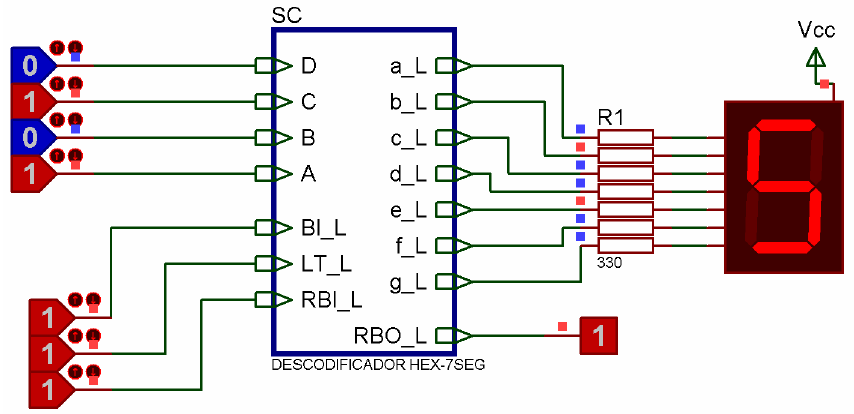
The analysis of simple digital circuits involves determining the circuit's behavior, which is represented by its truth table. To achieve this, the analysis can be organized step by step. For example, consider the circuit from EX1A's Fig. 2b. Note that...
Digital Circuits
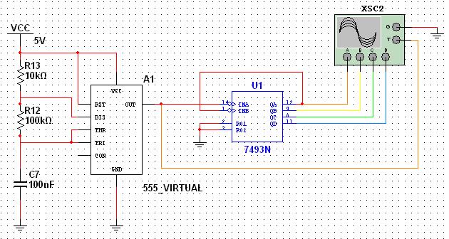
This tutorial explores a common digital concept using the NI Multisim software environment. It examines a four-bit counter that uses a 555 timer IC to generate the clock signal. This tutorial takes less than 30 minutes to complete and consists...
LOGIC DESIGNER
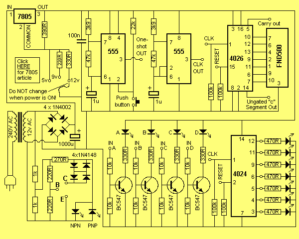
The logic designer is filled with features. It would not be possible to list all the possible combinations of the unit as the various building blocks on the board can be interconnected to obtain a wide variety of counting and...
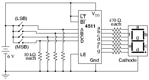
Lessons on Electric Circuits Experiments
Digital circuits are circuits that handle signals restricted to binary states of zero and a maximum value. This is in contrast to analog circuits, where signals can vary continuously within the limits set by power supply voltage and circuit resistances....
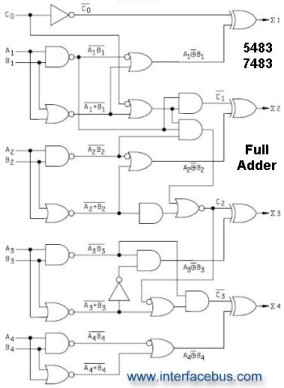
IC Adder Chip
A 4-bit adder adds two four-bit binary numbers along with a carry-in line. The accompanying diagram illustrates the logic gate schematic of a 4-bit adder. A full adder accepts two inputs and a carry-in line, while a half adder does...
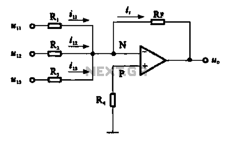
Adder circuit
An adder circuit, specifically the inverting adder circuit, utilizes the inverting input of an operational amplifier to process signals. Voltage inputs are added through resistors connected to the inverting input terminal of the operational amplifier. The circuit configuration, as depicted...