


DTL internal structure of the inverter circuit
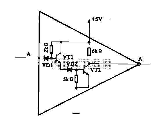
Description: The internal structure of the DTL inverter circuit (M5936P) is composed of inputs with diodes and transistors for signal processing, powered by a +5V supply. When the input terminal A is at a high level (digital 1), diode VDI is off, transistor VT1 is turned on, and transistor VT2 conducts, resulting in a low output (digital 0). Conversely, when the input is low (digital 0), diode VD1 conducts, transistor VT1 is off, and transistor VT2 is also off, leading to a high output (digital 1).
The M5936P DTL (Diode-Transistor Logic) inverter circuit utilizes a combination of diodes and bipolar junction transistors (BJTs) to perform its logical operations. The circuit is powered by a +5V supply, which is standard for digital logic circuits, ensuring compatibility with other digital components.
In the high input state, where terminal A receives a logic high (digital 1), diode VDI becomes reverse-biased, preventing current flow through it. Concurrently, this condition allows transistor VT1 to turn on, which then drives the base of transistor VT2. As a result, transistor VT2 enters saturation, allowing current to flow from the collector to the emitter, thus producing a low output state (digital 0) at the output terminal.
In contrast, when the input state is low (digital 0), diode VD1 becomes forward-biased, allowing current to flow through it. This action turns off transistor VT1, which in turn keeps transistor VT2 in the off state as well. Consequently, the output terminal reflects a high state (digital 1), indicating that no current flows through the output.
This inverter circuit exemplifies the fundamental operation of DTL logic, where the combination of diodes and transistors effectively implements logical inversion. The design is efficient for small signal processing applications and can be integrated into larger DTL logic families for more complex digital systems. The simplicity of the inverter circuit allows for easy expansion and incorporation into various digital applications while maintaining reliability and performance.DTL internal structure shown in the inverter circuit (M5936P) is. Inputs with diodes, transistors signal processing, power supply is + 5V. When the input terminal A high level (digital I ) when the diode VDI off, VTI transistor is turned on, the transistor VT2 conduction output is low (digital O ). When the input is low (the number 0 ), the diode VD1 conduction, transistor VT1 off, transistor VT2 off, output high (the number 1 ).
The M5936P DTL (Diode-Transistor Logic) inverter circuit utilizes a combination of diodes and bipolar junction transistors (BJTs) to perform its logical operations. The circuit is powered by a +5V supply, which is standard for digital logic circuits, ensuring compatibility with other digital components.
In the high input state, where terminal A receives a logic high (digital 1), diode VDI becomes reverse-biased, preventing current flow through it. Concurrently, this condition allows transistor VT1 to turn on, which then drives the base of transistor VT2. As a result, transistor VT2 enters saturation, allowing current to flow from the collector to the emitter, thus producing a low output state (digital 0) at the output terminal.
In contrast, when the input state is low (digital 0), diode VD1 becomes forward-biased, allowing current to flow through it. This action turns off transistor VT1, which in turn keeps transistor VT2 in the off state as well. Consequently, the output terminal reflects a high state (digital 1), indicating that no current flows through the output.
This inverter circuit exemplifies the fundamental operation of DTL logic, where the combination of diodes and transistors effectively implements logical inversion. The design is efficient for small signal processing applications and can be integrated into larger DTL logic families for more complex digital systems. The simplicity of the inverter circuit allows for easy expansion and incorporation into various digital applications while maintaining reliability and performance.DTL internal structure shown in the inverter circuit (M5936P) is. Inputs with diodes, transistors signal processing, power supply is + 5V. When the input terminal A high level (digital I ) when the diode VDI off, VTI transistor is turned on, the transistor VT2 conduction output is low (digital O ). When the input is low (the number 0 ), the diode VD1 conduction, transistor VT1 off, transistor VT2 off, output high (the number 1 ).

metal detector circuit
This circuit diagram represents a low-cost metal detector utilizing a single transistor circuit in conjunction with an old pocket radio. It operates as a Colpitts oscillator functioning within the medium band frequency range, with the radio tuned to the same...
Recording signal amplifying transistor circuit
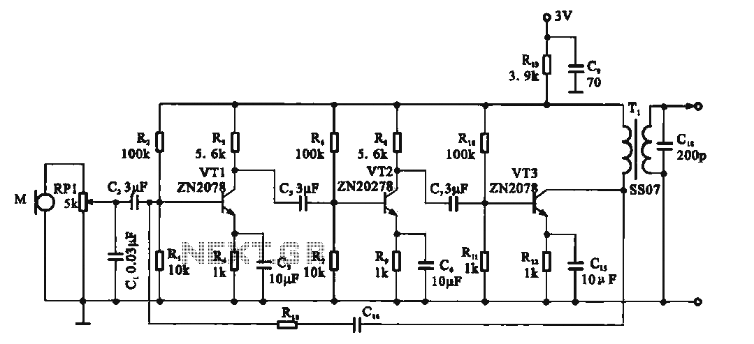
This circuit is a recording signal amplifying transistor circuit that illustrates the functioning of a microphone signal amplifier. After adjustment through potentiometer RP1, the signal is applied to the transistor VT1, which operates as a common emitter amplifier. The emitter...
Voice amplifier transistor
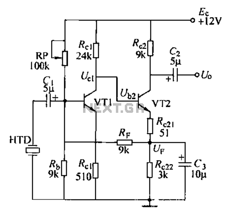
Dctl is a two-stage amplifier, with the first stage amplifying the collector voltage of transistor VT1. The second stage, represented by VT2, is proportional to the current flowing through the winding. The RF signal is applied to the sub-base of...
Simple 5V power supply for digital circuits
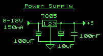
This circuit is a small +5V power supply, which is useful when experimenting with digital electronics. Small inexpensive wall transformers with variable output voltage are available from any electronics shop and supermarket. Those transformers are easily available, but usually their...
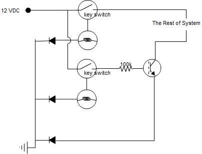
transistor as a switch circuit problems
A circuit is being designed that incorporates two key switches, which must both be closed for current to flow through the circuit.
The proposed circuit configuration employs two key switches connected in series. In this arrangement, the current can only pass...
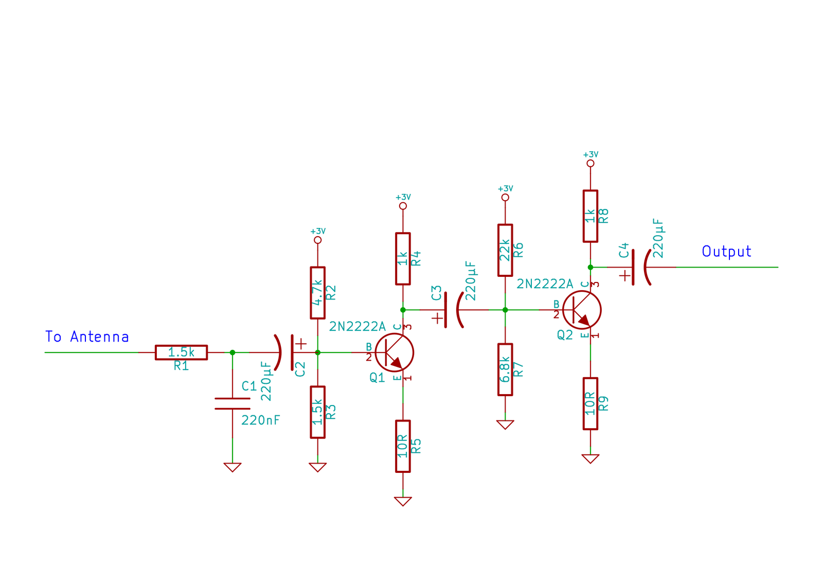
Simple Transistor Amplifier Circuit Schematic and Explanation
This circuit does not function as effectively as it could. It was created when the designer had a limited understanding of circuit design. An improved schematic will be developed and posted later, featuring a better design. The schematic indicates "antenna,"...
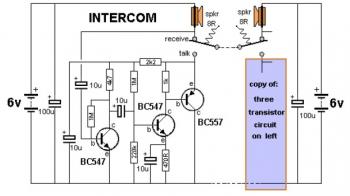
simple intercom circuit with
This is a two-station simple intercom circuit built using transistors and common 8-ohm mini speakers. The speaker functions as a microphone and generates sound, eliminating the need for a separate microphone in this intercom setup. The "press-to-talk" switches should have...
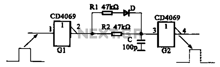
And broadening the delay circuit
The inverter circuit using CD4069 is configured with a delay and width adjustment. When the output of the inverter (G1) is high, the capacitor (C) charges through resistor (R1) and diode (D). The voltage across capacitor C quickly reaches the...
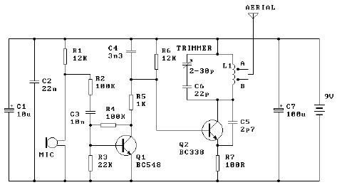
9V fm transmitter circuit design using transistors
The tuned coil L1 has two output tap points for the antenna connection, labeled "A" and "B." Both outputs are low-level, allowing the user to select between a stable low range or a more unstable but higher range. Tap B...