


Electronic CD4017 CD4066 the switch circuit diagram
#CD4017
#CD4066
#switch circuit
#digital switch
#logic IC
#electronic switch
#counter
#CMOS
#sequential logic
#circuit diagram
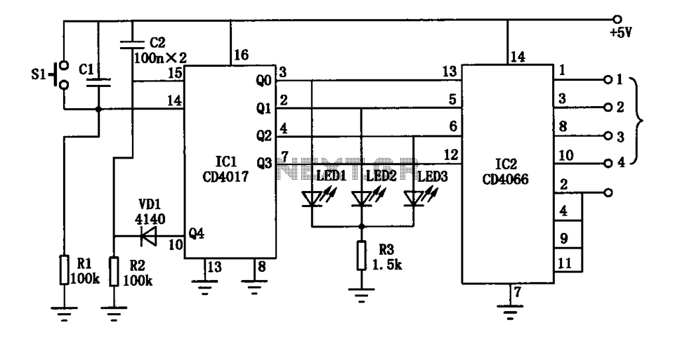
Description: The electronic circuit diagram consists of the CD4017 and CD4066 components configured as a switch circuit.
The CD4017 is a decade counter integrated circuit (IC) that can drive up to ten outputs, sequentially activating them based on clock pulses. It is commonly used in applications requiring counting and sequencing. Each output pin (Q0 to Q9) goes high in response to a clock signal, allowing for the control of various devices or circuits.
The CD4066 is a quad bilateral switch IC that can control analog or digital signals. It contains four independent switches that can be used to connect or disconnect signals from a circuit. The switches are controlled by digital signals, allowing for versatile applications in signal routing and manipulation.
In the switch circuit diagram utilizing both the CD4017 and CD4066, the output pins of the CD4017 can be connected to the control inputs of the CD4066 switches. This configuration allows the activation of specific switches based on the counting sequence of the CD4017. For instance, as the CD4017 counts from 0 to 9, it can enable different paths in the circuit, effectively routing signals through the CD4066 switches.
To implement this circuit, the CD4017 would be connected to a clock source, which could be a simple oscillator circuit generating pulses. The outputs of the CD4017 would then connect to the control pins of the CD4066. The input signals to the CD4066 would be routed from the source, and the outputs could lead to various destinations, such as LEDs, motors, or other electronic components.
This configuration allows for dynamic control of multiple outputs using a single clock signal, making it ideal for applications in timing, sequencing, or automated control systems. The combination of the CD4017 and CD4066 provides a flexible and efficient means of managing multiple signal paths in electronic designs.Electronic CD4017, CD4066 constitute the switch circuit diagram:
The CD4017 is a decade counter integrated circuit (IC) that can drive up to ten outputs, sequentially activating them based on clock pulses. It is commonly used in applications requiring counting and sequencing. Each output pin (Q0 to Q9) goes high in response to a clock signal, allowing for the control of various devices or circuits.
The CD4066 is a quad bilateral switch IC that can control analog or digital signals. It contains four independent switches that can be used to connect or disconnect signals from a circuit. The switches are controlled by digital signals, allowing for versatile applications in signal routing and manipulation.
In the switch circuit diagram utilizing both the CD4017 and CD4066, the output pins of the CD4017 can be connected to the control inputs of the CD4066 switches. This configuration allows the activation of specific switches based on the counting sequence of the CD4017. For instance, as the CD4017 counts from 0 to 9, it can enable different paths in the circuit, effectively routing signals through the CD4066 switches.
To implement this circuit, the CD4017 would be connected to a clock source, which could be a simple oscillator circuit generating pulses. The outputs of the CD4017 would then connect to the control pins of the CD4066. The input signals to the CD4066 would be routed from the source, and the outputs could lead to various destinations, such as LEDs, motors, or other electronic components.
This configuration allows for dynamic control of multiple outputs using a single clock signal, making it ideal for applications in timing, sequencing, or automated control systems. The combination of the CD4017 and CD4066 provides a flexible and efficient means of managing multiple signal paths in electronic designs.Electronic CD4017, CD4066 constitute the switch circuit diagram:
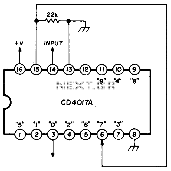
Cmos programmable divide-by-n counter
A single connection change allows division by any integer between 2 and 10. The RCA CD4017A Johnson decade counter is configured as a divide-by-7 counter. A resistor is utilized to maintain the reset line in a low state. When the...
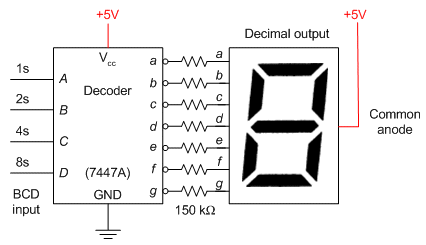
Debounced Counter Made From Off-The-Shelf Chips
The true utility of the SR latch is evident during transitions of the input switch. Assume that the input switch is of the break-before-make type and starts in the up position. When the switch is up, the input values are...
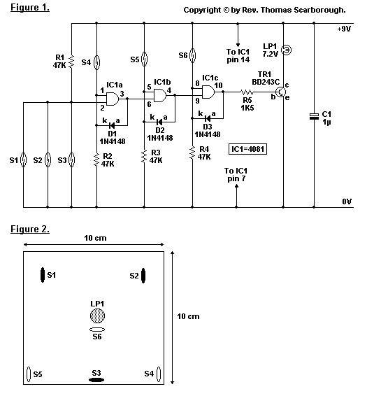
Magic Wand Conjuring Trick
The operation of the circuit is fairly simple. Three AND logic gates of a 4081 CMOS IC are employed, with gates IC1a to IC1c being configured as a standard cascaded latch circuit. S1 to S3 serve as reset switches. The...
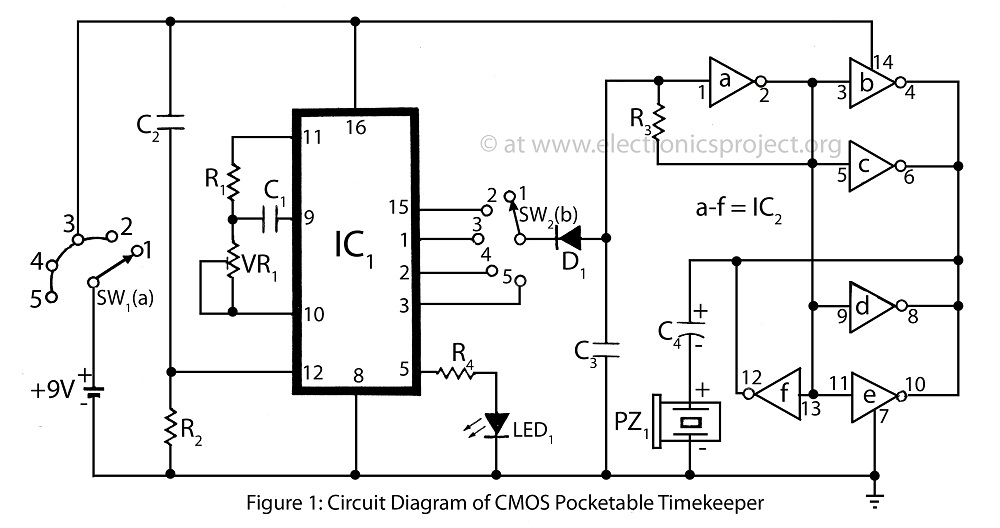
CMOS Pocketable Timekeeper
The CMOS Pocketable Timekeeper is a compact timekeeping circuit designed for portability. This circuit diagram illustrates the functionality of the CMOS Pocketable Timekeeper along with various advanced timer projects and electronic applications.
The CMOS Pocketable Timekeeper circuit utilizes complementary metal-oxide-semiconductor (CMOS)...
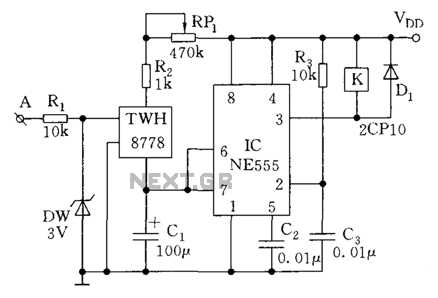
Optionally extended charging pulse count switch circuit diagram
The count switching circuit consists of an electronic switch and a pulse delay circuit for control.
The count switching circuit is designed to manage the switching of signals in a controlled manner. The electronic switch serves as the primary component for...
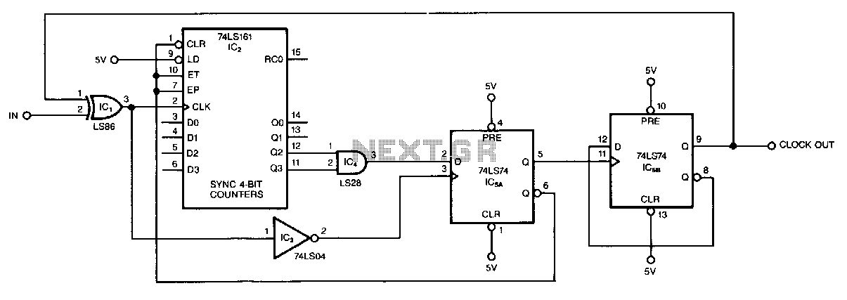
Odd-number-counter-divider
This circuit, illustrated symmetrically, divides an input by virtually any odd number. The circuit counts n + 1/2 clocks twice to achieve the desired divisor. By selecting the appropriate n, which is the decoded output of the LS161 counter, divisors...
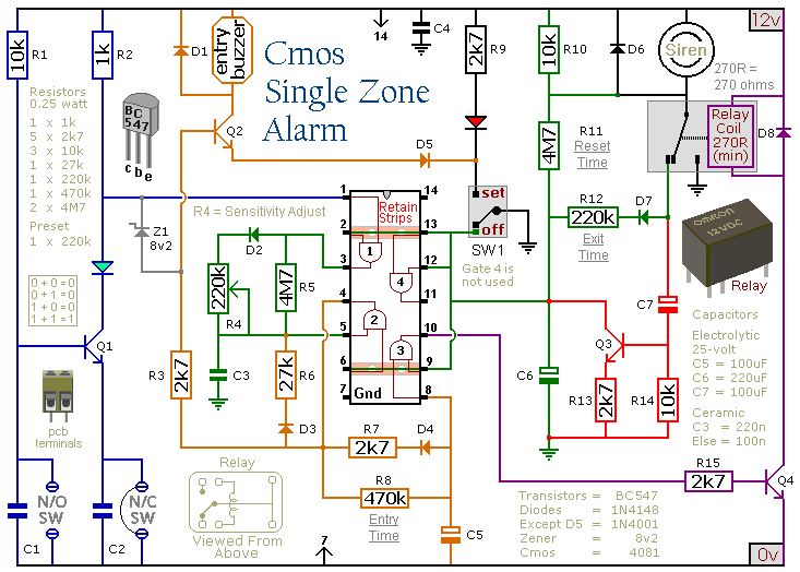
A Cmos Based Single Zone Alarm circuit
This circuit features automatic exit and entry delays, a timed bell cut-off, and a system reset. It accommodates both normally-open and normally-closed switches, making it compatible with various input devices such as pressure mats, magnetic reed contacts, foil tape, PIRs,...
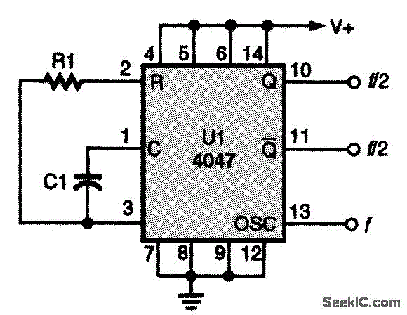
CD4047 CMOS OSCILLATOR
This CMOS square-wave oscillator utilizes the 4047 multivibrator circuit, suitable for both monostable (one-shot) and astable applications. In the provided configuration, the 4047 operates as an astable multivibrator. The circuit features three outputs from the 4047, with the first being...
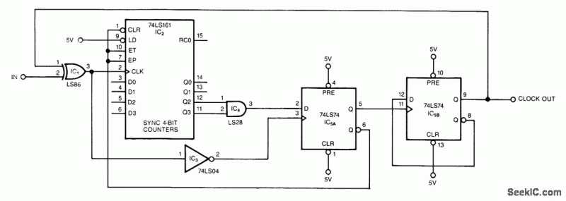
DIVIDE BY ODD NUMBER COUNTER
This circuit symmetrically divides an input by virtually any odd number. The circuit contains n+l/2 clocks twice to achieve the desired divisor. By selecting the proper n, which is the decoded output of the 74LS161 counter, divisors from 3 to...