


frequency doubler with 4069
#4069
#hex inverter
#frequency doubler
#squarewave
#pulse train
#digital IC
#logic circuits
#signal processing
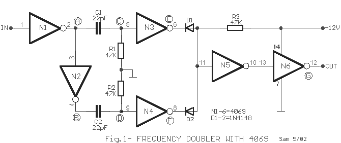
Description: A frequency doubler can be constructed using a single 4069 hex inverter IC, resulting in an output pulse train with a frequency that is twice that of the square wave input signal.
The frequency doubler circuit utilizing the 4069 hex inverter IC is an efficient method for generating a signal at double the frequency of the input. The 4069 is a quad inverter, which means it contains four independent inverter gates, allowing for versatile designs.
To construct the frequency doubler, the circuit typically consists of one inverter from the 4069 IC, connected to the input square wave signal. The output of this inverter is then fed into a second inverter, creating a feedback loop that generates oscillations. The feedback is achieved through a resistor-capacitor (RC) network, which determines the timing characteristics of the circuit.
The input square wave signal is applied to the first inverter, which inverts the signal. The output from the first inverter is then connected to an RC network, consisting of a resistor (R) and capacitor (C). This RC network introduces a phase shift that is crucial for frequency doubling. The output of the RC network is then fed into the second inverter, which further inverts the signal.
The result is a pulse train at the output that has a frequency that is twice that of the original input signal. The output can be observed using an oscilloscope, which will display a waveform with a frequency that is double that of the input square wave.
This frequency doubler circuit is useful in various applications, including signal processing, modulation, and clock generation in digital circuits. The simplicity of using a single IC makes it an attractive solution for designers looking to implement frequency doubling in their projects. Proper selection of the resistor and capacitor values is critical, as it affects the performance and stability of the frequency doubling process.This frequency doubler using a single 4069 hex inverter IC, a frequency doubler can be constructed to give an output pulse train whose frequency is twice that of a squarewave input signal..
The frequency doubler circuit utilizing the 4069 hex inverter IC is an efficient method for generating a signal at double the frequency of the input. The 4069 is a quad inverter, which means it contains four independent inverter gates, allowing for versatile designs.
To construct the frequency doubler, the circuit typically consists of one inverter from the 4069 IC, connected to the input square wave signal. The output of this inverter is then fed into a second inverter, creating a feedback loop that generates oscillations. The feedback is achieved through a resistor-capacitor (RC) network, which determines the timing characteristics of the circuit.
The input square wave signal is applied to the first inverter, which inverts the signal. The output from the first inverter is then connected to an RC network, consisting of a resistor (R) and capacitor (C). This RC network introduces a phase shift that is crucial for frequency doubling. The output of the RC network is then fed into the second inverter, which further inverts the signal.
The result is a pulse train at the output that has a frequency that is twice that of the original input signal. The output can be observed using an oscilloscope, which will display a waveform with a frequency that is double that of the input square wave.
This frequency doubler circuit is useful in various applications, including signal processing, modulation, and clock generation in digital circuits. The simplicity of using a single IC makes it an attractive solution for designers looking to implement frequency doubling in their projects. Proper selection of the resistor and capacitor values is critical, as it affects the performance and stability of the frequency doubling process.This frequency doubler using a single 4069 hex inverter IC, a frequency doubler can be constructed to give an output pulse train whose frequency is twice that of a squarewave input signal..
Pulse Train
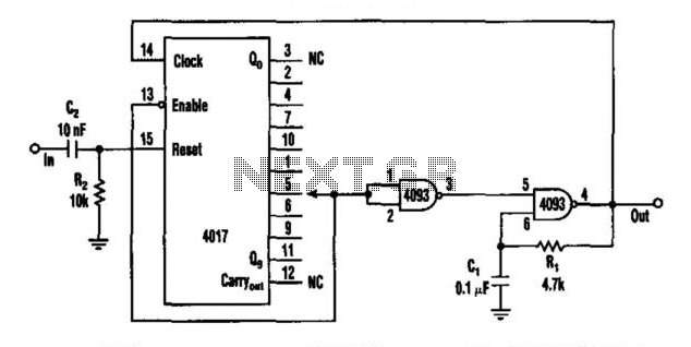
This circuit features a rate multiplier utilizing a 4093 Schmitt trigger configured as an oscillator, which drives a 4017 decade counter. When a pulse is present at the input (to C2), the 4017 is reset, causing output zero to go...
Pulse-Train Triggering Circuit for Power Control
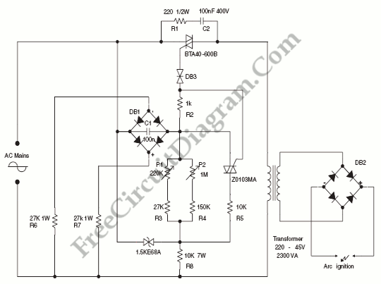
A typical circuit for welding equipment is illustrated in the following circuit diagram. The turn-on delay can be accurately controlled with Potentiometer P2, allowing for effective discharge management.
The welding equipment circuit typically incorporates several key components to ensure proper operation...
Door Knob alarm
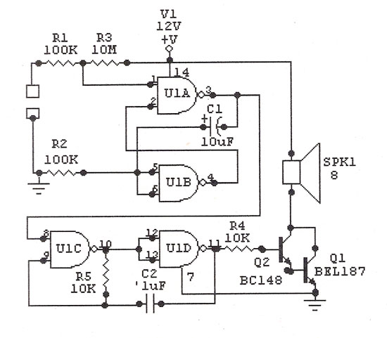
Digital IC Door Knob Alarm Circuit. This circuit activates an alarm when an object is touched. For example, if someone touches the door handle, an internal buzzer will sound.
The digital IC door knob alarm circuit is designed to enhance security...
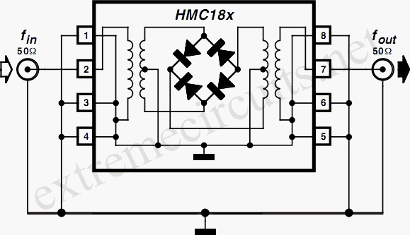
Frequency Doubler
When working with frequencies ranging from 850 MHz to 4 GHz, a frequency multiplier may be necessary. The HMC 187, HMC 188, and HMC 189 frequency doublers could be suitable solutions. These devices offer isolation performance that attenuates the input...
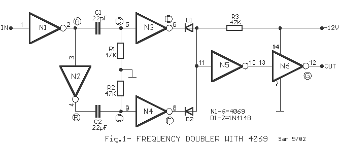
Frequency doubler
This frequency doubler using a single 4069 hex inverter IC, a frequency doubler can be constructed to give an output pulse train whose frequency is twice that of a squarewave input signal. The signal is applied to the input of...
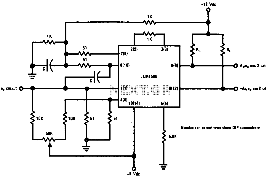
Broadband frequency doubler
This circuit is designed to double low-level signals while maintaining low distortion. The capacitor value (C) should be selected to ensure low reactance at the operating frequency. The signal level at the carrier input should remain below 25 mV peak...
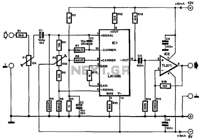
Audio-Frequency Doubler
Often, the frequency of a signal must be doubled, and the modulator/demodulator chip LM1496 serves as an ideal basis for this application. From trigonometry, it is well known that 2sin(x)cos(x) = sin(2x) and sin^2(x) = 1 - cos^2(x). These equations...
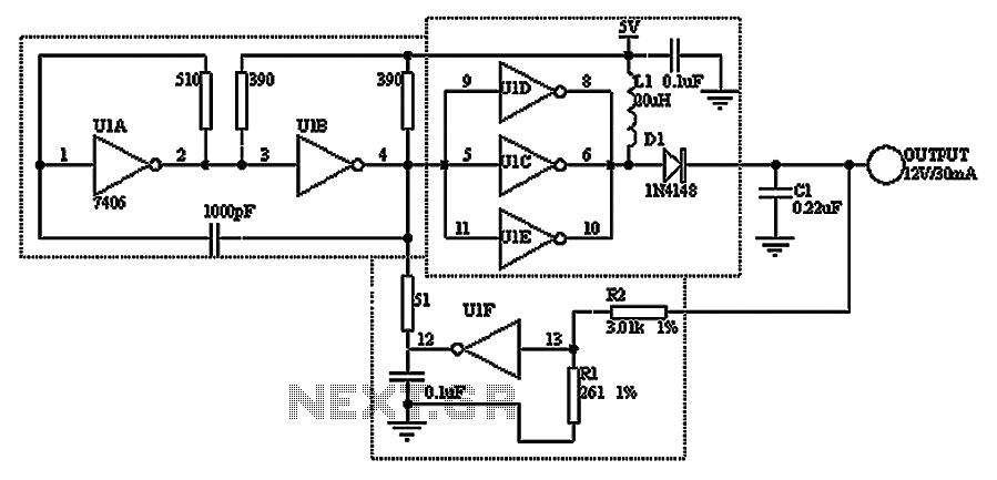
Made with hex inverter DC DC converter circuit
A TTL hex inverter circuit can function as a DC/DC converter, converting 5V to 12V. This circuit encompasses all necessary functionalities for DC/DC conversion. It relies on a TTL switching threshold voltage regulator. The components U1A and U1B form an...
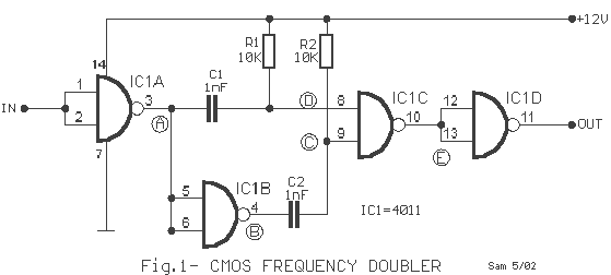
Frequency doubler II
This frequency doubler uses one CMOS quad, two input NAND gate package type 4011. The frequency doubler proper consists of an inverter IC1B, two differentiating networks R1/C1, R2/C2 and NAND gate IC1A, IC1C and IC1D function as input and output...