


Motorola SN54 Demultiplexer Logic Diagram and Datasheet
#demultiplexer
#decoder
#Motorola SN54
#74LS138
#logic diagram
#memory chip
#address decoding
#enable function
#parallel expansion
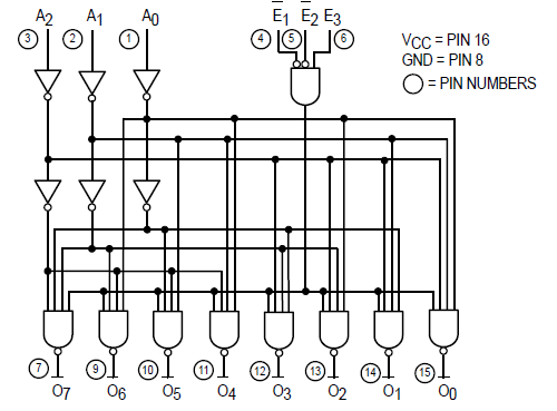
Description: The Motorola SN54/74LS138 is recognized as a 1-of-8 decoder or demultiplexer, specifically engineered for high-speed bar memory chip select address decoding. The accompanying diagram illustrates the logic configuration of the SN54/74LS138 demultiplexer. According to the SN54 datasheet, the multiple enable function facilitates straightforward parallel expansion of the device to create a 1-of-32 decoder (using 5 input lines to decode to 32 output lines) with the integration of four LS138 devices and one inverter.
The Motorola SN54/74LS138 is a high-speed CMOS logic device that operates as a 1-of-8 line decoder/demultiplexer. This component features three binary select inputs (A0, A1, A2) that can decode a 3-bit binary number into one of eight active low outputs (Y0 to Y7). The device also includes three enable inputs (G1, G2A, G2B) which must be appropriately activated to allow the decoder to function. When the enable inputs are not activated, all outputs remain inactive regardless of the select input states.
The operational speed of the SN54/74LS138 makes it suitable for applications requiring rapid address decoding, such as in memory chip selection for microprocessors. The architecture of the device allows for cascading multiple SN54/74LS138 chips to expand the decoding capability. By connecting four of these devices along with a single inverter, one can achieve a 1-of-32 decoding scheme. This is accomplished by using five input lines to select one of the thirty-two outputs, effectively increasing the number of selectable outputs while maintaining the high-speed performance characteristic of the SN54/74LS138.
In practical applications, the multiple enable function enhances versatility in circuit design, allowing for complex configurations without significant additional components. The logic diagram of the SN54/74LS138 can be utilized to understand the internal workings of the device, including the AND gates and inverters used to produce the desired output based on the binary input. This makes the SN54/74LS138 a crucial component in digital systems requiring efficient address decoding and demultiplexing capabilities.Motorola SN54/74LS138 known to be 1-of-8 decoder or demultiplexer which is designed for high speed bar memory chip select address decoding. Below diagram illustrates logic diagram of this SN54/74LS138 demultiplexer. According to the SN54 datasheet, multiple enable function allows easy parallel expansion of the device to a 1-of-32 (5 lines to 32 li
nes) decoder with just four LS138s and one inverter. Diagram
The Motorola SN54/74LS138 is a high-speed CMOS logic device that operates as a 1-of-8 line decoder/demultiplexer. This component features three binary select inputs (A0, A1, A2) that can decode a 3-bit binary number into one of eight active low outputs (Y0 to Y7). The device also includes three enable inputs (G1, G2A, G2B) which must be appropriately activated to allow the decoder to function. When the enable inputs are not activated, all outputs remain inactive regardless of the select input states.
The operational speed of the SN54/74LS138 makes it suitable for applications requiring rapid address decoding, such as in memory chip selection for microprocessors. The architecture of the device allows for cascading multiple SN54/74LS138 chips to expand the decoding capability. By connecting four of these devices along with a single inverter, one can achieve a 1-of-32 decoding scheme. This is accomplished by using five input lines to select one of the thirty-two outputs, effectively increasing the number of selectable outputs while maintaining the high-speed performance characteristic of the SN54/74LS138.
In practical applications, the multiple enable function enhances versatility in circuit design, allowing for complex configurations without significant additional components. The logic diagram of the SN54/74LS138 can be utilized to understand the internal workings of the device, including the AND gates and inverters used to produce the desired output based on the binary input. This makes the SN54/74LS138 a crucial component in digital systems requiring efficient address decoding and demultiplexing capabilities.Motorola SN54/74LS138 known to be 1-of-8 decoder or demultiplexer which is designed for high speed bar memory chip select address decoding. Below diagram illustrates logic diagram of this SN54/74LS138 demultiplexer. According to the SN54 datasheet, multiple enable function allows easy parallel expansion of the device to a 1-of-32 (5 lines to 32 li
nes) decoder with just four LS138s and one inverter. Diagram
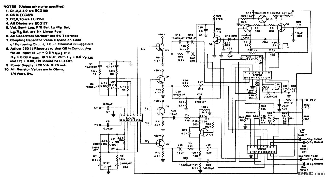
4-channel SQ logic decoder
4-channel SQ logic decoder with a current drain of 75 mA at 20 volts. The input impedance is 2M ohms, and the output impedance is 2K ohms (courtesy of GTE Sylvania Incorporated).
The 4-channel SQ logic decoder is an integrated circuit...
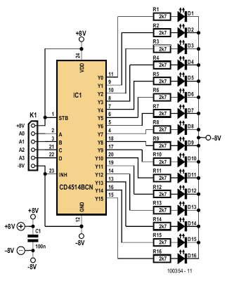
Simple Indicator for Dynamic Limiter Schematic Diagram
The indicator described here is specifically designed for adjusting the dynamic limiter outlined elsewhere in this edition and checking if the maximum level of the reference voltage (P1) requires modification. A 4-to-16 decoder integrated circuit (IC) of type 4514 is...
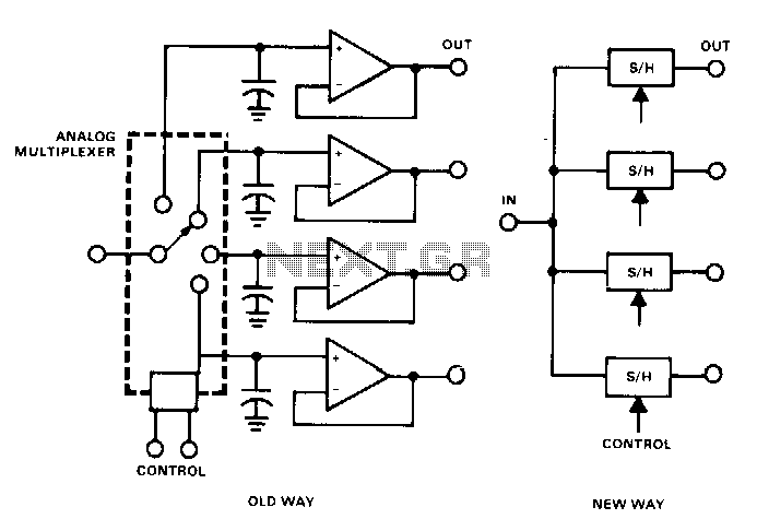
Demultiplexer
This circuit reconstructs and separates analog signals that have been time-division multiplexed. The conventional method has several restrictions, particularly when a short dwell time and a long, accurate hold time are required. The capacitors must charge from a low-impedance source...
decoder
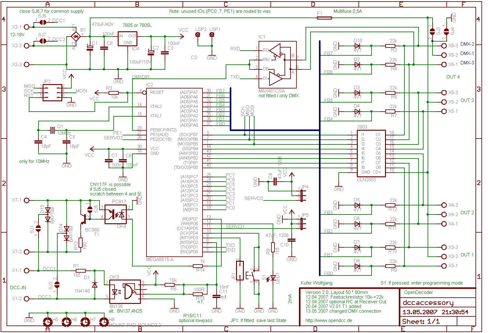
There is a version without SMD, referred to as version 2.1, which is slightly larger (80 x 100 mm) and features dual drivers capable of handling a 1A load. It operates using the same software. The input voltage from the...
Background music decoder
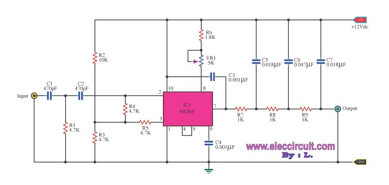
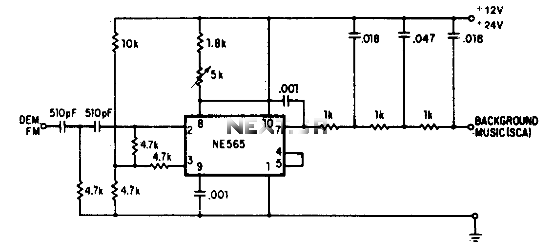
This circuit is a background music (SCA) decoder designed to process an input demodulated (multiplex) FM signal. The NE565, a Phase Locked Loop (PLL) integrated circuit, serves as the foundation for this design.
The background music (SCA) decoder circuit utilizes the...
A practical MS Decoder Circuit
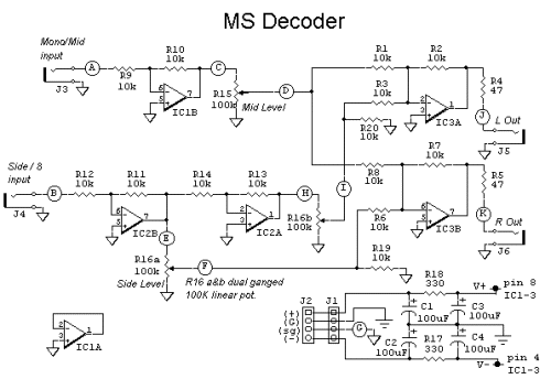
The schematic diagram of the MS Decoder may appear complex, but it is relatively straightforward. Initially, both the Mid and Side signals are buffered using unity gain inverting buffers, which are constructed around IC1b and IC2b. This buffering serves two...
decoder circuit
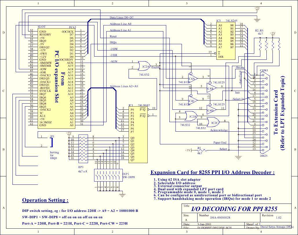
The PPI-8255 is a general-purpose I/O programmable interface that is typically connected directly to a computer bus. This article demonstrates that the card can serve dual purposes: as an expander port and for direct I/O functionality. The card can be...
low power universal demultiplexer decoder
This circuit functions as a universal decoder, capable of operating either as a dual 1-of-4 decoder or as a single 1-of-8 decoder, depending on the signal applied to the Mode Control (M) input. In the dual mode, each section features...
Sca background music decoder
A resistive voltage divider is utilized to establish a bias voltage for the input (pins 2 and 3). The demodulated FM signal is introduced to the input through a two-stage high-pass filter, which serves to provide capacitive coupling and to...